a 4-channel time interleaved sampler based 3-5 ghz band ... · 88 sang gyun kim et al : a 4-channel...
TRANSCRIPT
JOURNAL OF SEMICONDUCTOR TECHNOLOGY AND SCIENCE, VOL.18, NO.1, FEBRUARY, 2018 ISSN(Print) 1598-1657 https://doi.org/10.5573/JSTS.2018.18.1.084 ISSN(Online) 2233-4866
Manuscript received Jun. 6, 2017; accepted Dec. 7, 2017 1 Department of Electronic Engineering, Kwang-woon University. 2 Dept. of Electronic and IT Media Engineering, Seoul National University of Science and Technology E-mail : [email protected] (Corresponding Author : Hyung Chul Park)
A 4-channel Time Interleaved Sampler based 3-5 GHz band CMOS Radar IC in 0.13 mm for Surveillance
Sang Gyun Kim1, Yun Seong Eo1, and Hyung Chul Park2
Abstract—This paper presents a 3-5 GHz band CMOS UWB radar IC realized in a 0.13 mm CMOS technology for surveillance. Sampling resolution and detectable range of the proposed IC are determined to be 3 cm and 15 m, respectively, to serve a surveillance function. To reduce the scan time while satisfying resolution and detection range, equivalent time sampling and a 4-channel time interleaved sampler are used. The DC offset mismatch in the 4-channel receiver is greatly reduced via a DC offset compensation and BJT-based op-amp for analog signal processing (ASP) circuits. Measurement results show that the center frequency and bandwidth of the pulse can be adjusted in the range of 3 GHz - 5 GHz and 0.5 GHz - 2 GHz, respectively. The measured range for human target is up to 11 m. The chip size is 4 mm ´ 2.5 mm, and 81 mA (transmitter) and 38 mA (receiver) are consumed at 1.5 V supply. Index Terms—CMOS single chip radar, UWB pulse radar, DC offset compensation, digitally synthesized impulse generator
I. INTRODUCTION
As the demand for high-resolution radar increases, ultra wideband (UWB) radar is considered a good solution for many civilian and military applications such
as localization and biometric imaging. Recent studies have presented CMOS UWB IC-based radars for sensor applications [1-4]. In [1], since an analog detection technique was used, performance improvement using digital signal processing (DSP) technique may not be much. In [2], CMOS UWB radar IC used equivalent time sampling technique and 16-channel time interleaved samplers; however, the IC has many problems such as circuit saturation due to DC offset and channel-to-channel equalization.
This paper presents a 3–5 GHz band CMOS UWB radar IC for surveillance. The proposed IC is fabricated in a 0.13 mm technology. To serve a surveillance function, sampling resolution and detection range of the proposed IC are determined to be 3 cm and 15 m, respectively. To reduce the scan time while satisfying resolution and detection range, equivalent time sampling and a 4-channel time interleaved sampler are used. This paper is organized as follows: In Section II, we present the system architecture of the proposed IC. In Section III, the circuit design of the IC is presented. The measurement results are presented in section IV and conclusions are presented in Section V.
II. SYSTEM ARCHITECTURE
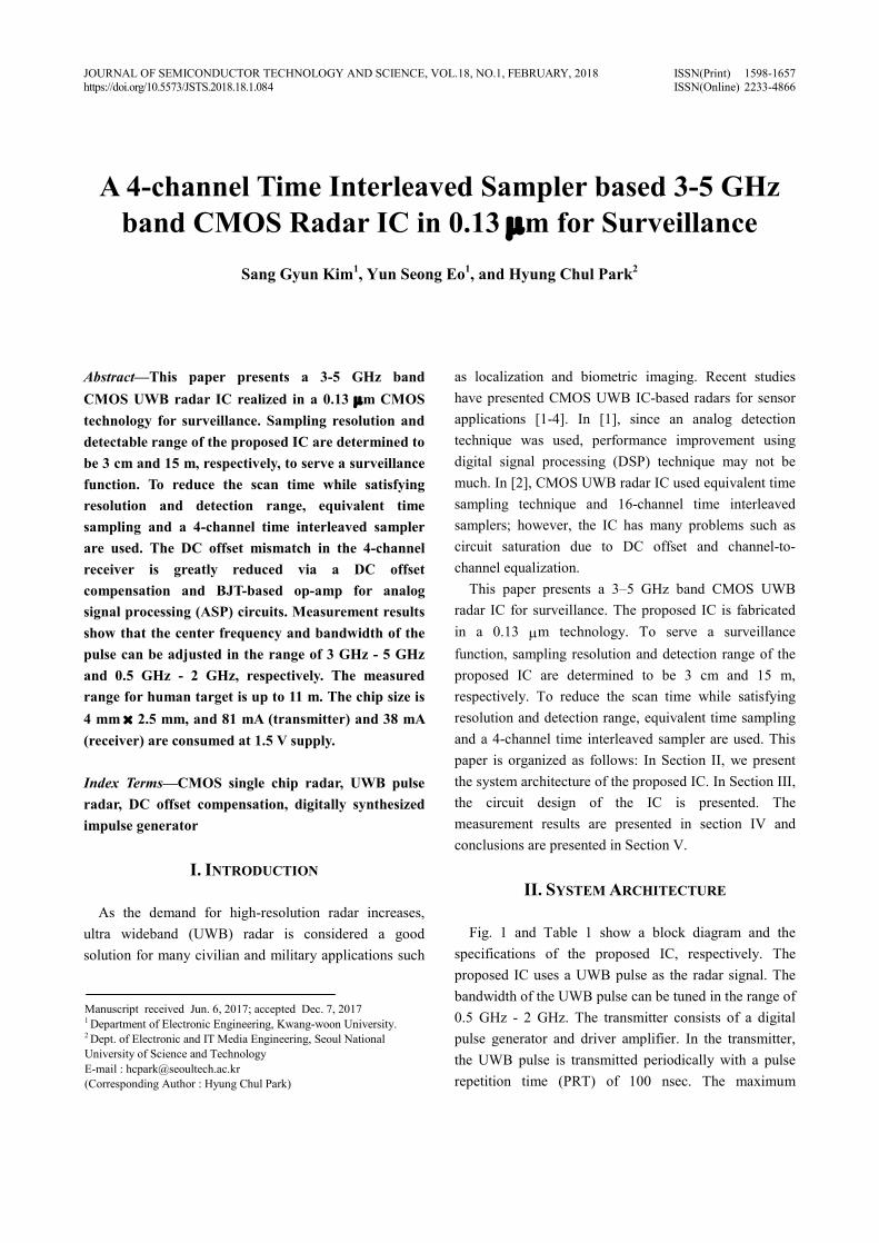
Fig. 1 and Table 1 show a block diagram and the specifications of the proposed IC, respectively. The proposed IC uses a UWB pulse as the radar signal. The bandwidth of the UWB pulse can be tuned in the range of 0.5 GHz - 2 GHz. The transmitter consists of a digital pulse generator and driver amplifier. In the transmitter, the UWB pulse is transmitted periodically with a pulse repetition time (PRT) of 100 nsec. The maximum
JOURNAL OF SEMICONDUCTOR TECHNOLOGY AND SCIENCE, VOL.18, NO.1, FEBRUARY, 2018 85
transmission power is -41.3 dBm/MHz. The receiver consists of a low-noise amplifier (LNA), single to differential (S2D) amplifier, RF variable gain amplifier (VGA), 4-way RF power splitter, four analog signal processing (ASP) blocks, and two delay-locked loops (DLLs). The single-ended output of the LNA is converted to differential signals using the S2D amplifier. The RF VGA output is divided using a 4-way power splitter. In each ASP block, the VGA and integrator circuit amplifies and integrates the received small signal to enhance the signal-to-noise ratio (SNR). Finally, sample-and-hold (S/H) circuit produces the stair-step waveform for the external analog-to-digital converter (ADC) and DSP.
The receiver utilizes equivalent time sampling and 4-channel time interleaved sampling techniques. The use of a four-channel architecture is decided on by considering the complexity and difficulty of the equalizer and detection resolution. Since the PRT is equal to 100 nsec, the scan time and detection range are equal to 100 nsec and 15 m, respectively. Since detection range
, the scan time range of 100 nsec is divided into 500 bins, which individually
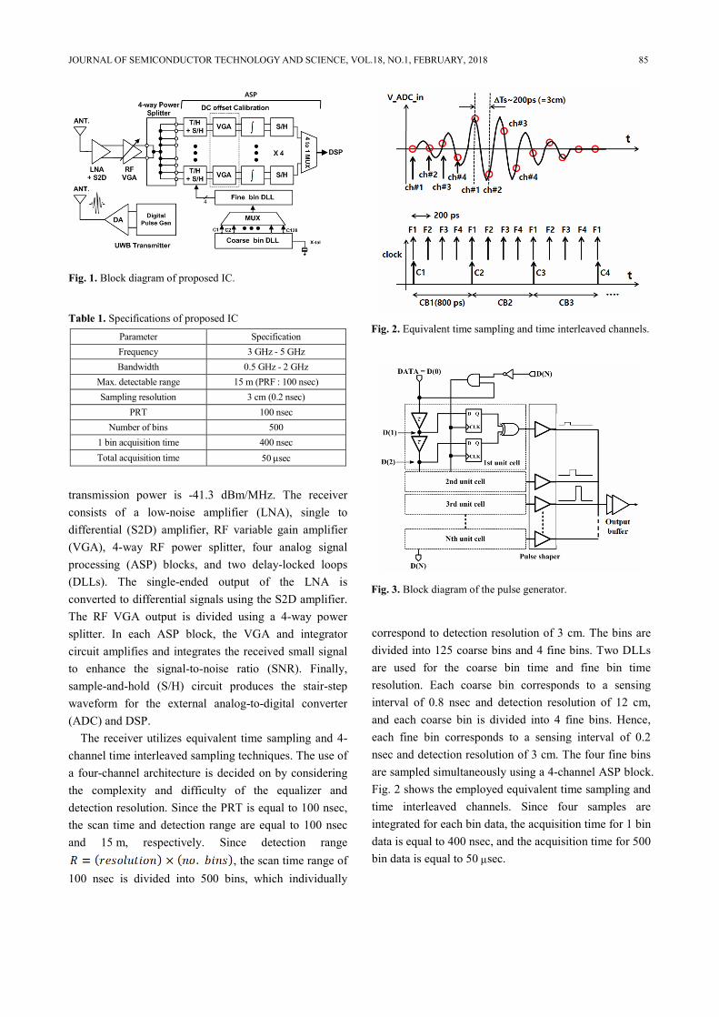
correspond to detection resolution of 3 cm. The bins are divided into 125 coarse bins and 4 fine bins. Two DLLs are used for the coarse bin time and fine bin time resolution. Each coarse bin corresponds to a sensing interval of 0.8 nsec and detection resolution of 12 cm, and each coarse bin is divided into 4 fine bins. Hence, each fine bin corresponds to a sensing interval of 0.2 nsec and detection resolution of 3 cm. The four fine bins are sampled simultaneously using a 4-channel ASP block. Fig. 2 shows the employed equivalent time sampling and time interleaved channels. Since four samples are integrated for each bin data, the acquisition time for 1 bin data is equal to 400 nsec, and the acquisition time for 500 bin data is equal to 50 msec.
ASP
4
Fig. 1. Block diagram of proposed IC.
Table 1. Specifications of proposed IC
Parameter Specification Frequency 3 GHz - 5 GHz Bandwidth 0.5 GHz - 2 GHz
Max. detectable range 15 m (PRF : 100 nsec) Sampling resolution 3 cm (0.2 nsec)
PRT 100 nsec Number of bins 500
1 bin acquisition time 400 nsec Total acquisition time 50 msec
Fig. 2. Equivalent time sampling and time interleaved channels.
Fig. 3. Block diagram of the pulse generator.
86 SANG GYUN KIM et al : A 4-CHANNEL TIME INTERLEAVED SAMPLER BASED 3-5 GHz BAND CMOS RADAR IC IN 0.13 mm …
III. CIRCUIT DESIGN
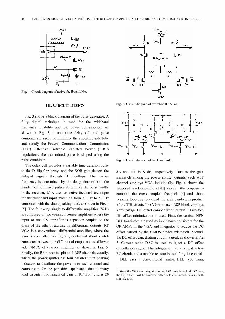
Fig. 3 shows a block diagram of the pulse generator. A fully digital technique is used for the wideband frequency tunability and low power consumption. As shown in Fig. 3, a unit time delay cell and pulse combiner are used. To minimize the undesired side lobe and satisfy the Federal Communications Commission (FCC) Effective Isotropic Radiated Power (EIRP) regulations, the transmitted pulse is shaped using the pulse combiner.
The delay cell provides a variable time duration pulse to the D flip-flop array, and the XOR gate detects the delayed signals through D flip-flops. The carrier frequency is determined by the delay time (τ) and the number of combined pulses determines the pulse width. In the receiver, LNA uses an active feedback technique for the wideband input matching from 3 GHz to 5 GHz combined with the shunt peaking load, as shown in Fig. 4 [5]. The following single to differential amplifier (S2D) is composed of two common source amplifiers where the input of one CS amplifier is capacitor coupled to the drain of the other, resulting in differential outputs. RF VGA is a conventional differential amplifier, where the gain is controlled via digitally-controlled shunt switch connected between the differential output nodes of lower side NMOS of cascade amplifier as shown in Fig. 5. Finally, the RF power is split to 4 ASP channels equally, where the power splitter has four parallel shunt peaking inductors to distribute the power into each channel and compensate for the parasitic capacitance due to many load circuits. The simulated gain of RF front end is 20
dB and NF is 8 dB, respectively. Due to the gain mismatch among the power splitter outputs, each ASP channel employs VGA individually. Fig. 6 shows the proposed track-and-hold (T/H) circuit. We propose to combine the cross coupled feedback [6] and shunt peaking topology to extend the gain bandwidth product of the T/H circuit. The VGA in each ASP block employs a front-stage DC offset compensation circuit.1 Two-fold DC offset minimization is used. First, the vertical NPN BJT transistors are used as input stage transistors for the OP-AMPs in the VGA and integrator to reduce the DC offset caused by the CMOS device mismatch. Second, the DC offset cancellation circuit is used, as shown in Fig. 7. Current mode DAC is used to inject a DC offset cancellation signal. The integrator uses a typical active RC circuit, and a tunable resistor is used for gain control.
DLL uses a conventional analog DLL type using
1 Since the VGA and integrator in the ASP block have high DC gain, the DC offset must be removed either before or simultaneously with amplification.
Fig. 4. Circuit diagram of active feedback LNA.
Fig. 5. Circuit diagram of switched RF VGA.
Fig. 6. Circuit diagram of track and hold.
JOURNAL OF SEMICONDUCTOR TECHNOLOGY AND SCIENCE, VOL.18, NO.1, FEBRUARY, 2018 87
voltage controlled delay line (VCDL) cell. The external 10 MHz clock is used as the reference clock for the coarse bin DLL. Fine bin DLL uses one of the output clocks of coarse bin DLL as the reference clock for the fine bin DLL.
IV. MEASUREMENT RESULTS
Fig. 8 shows a microphotograph of the fabricated UWB radar IC. The UWB radar IC is implemented using a 0.13 mm CMOS process, and the chip size is 4 mm ´ 2.5 mm. Fig. 9 shows the measured spectrum of the UWB pulse generator output. In Fig. 9, we find that the center frequency is variable from 3 GHz to 5 GHz. The tunable frequency step is 0.5 GHz. In the actual operation, the useful center frequency ranges from 3.5 GHz to 4.5 GHz for satisfying the spectrum mask requirement. Fig. 10 shows the measured waveform of the UWB pulse generator output. In Fig. 10, we find that the bandwidth can be adjusted between 500 MHz and 2 GHz with 500 MHz step.
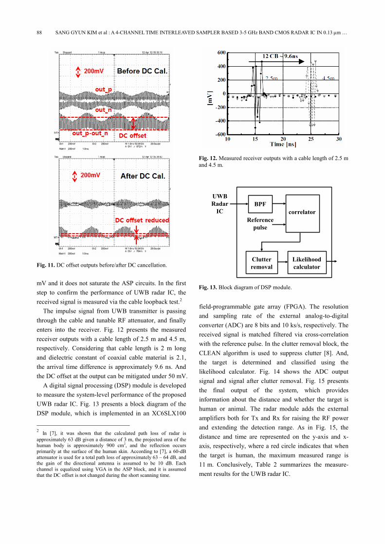
To avoid the saturation of ASP circuits, DC offset should be cancelled and suppressed sufficiently. Fig. 11 shows the DC offset reduction of differential output voltages of ASP block after DC offset cancellation. The DC offset voltage after calibration is suppressed under 50
Fig. 7. Circuit diagram of DC offset cancellation.
4 ch. ASPReceiver
RF front end
DLLPulse
generator
Fig. 8. Photo of fabricated UWB radar IC.
Fig. 9. Measured spectrum of UWB pulse generator output.
(a) 500 MHz
(b) 1 GHz
(c) 2 GHz
Fig. 10. Measured waveform of UWB pulse generator output.
88 SANG GYUN KIM et al : A 4-CHANNEL TIME INTERLEAVED SAMPLER BASED 3-5 GHz BAND CMOS RADAR IC IN 0.13 mm …
mV and it does not saturate the ASP circuits. In the first step to confirm the performance of UWB radar IC, the received signal is measured via the cable loopback test.2
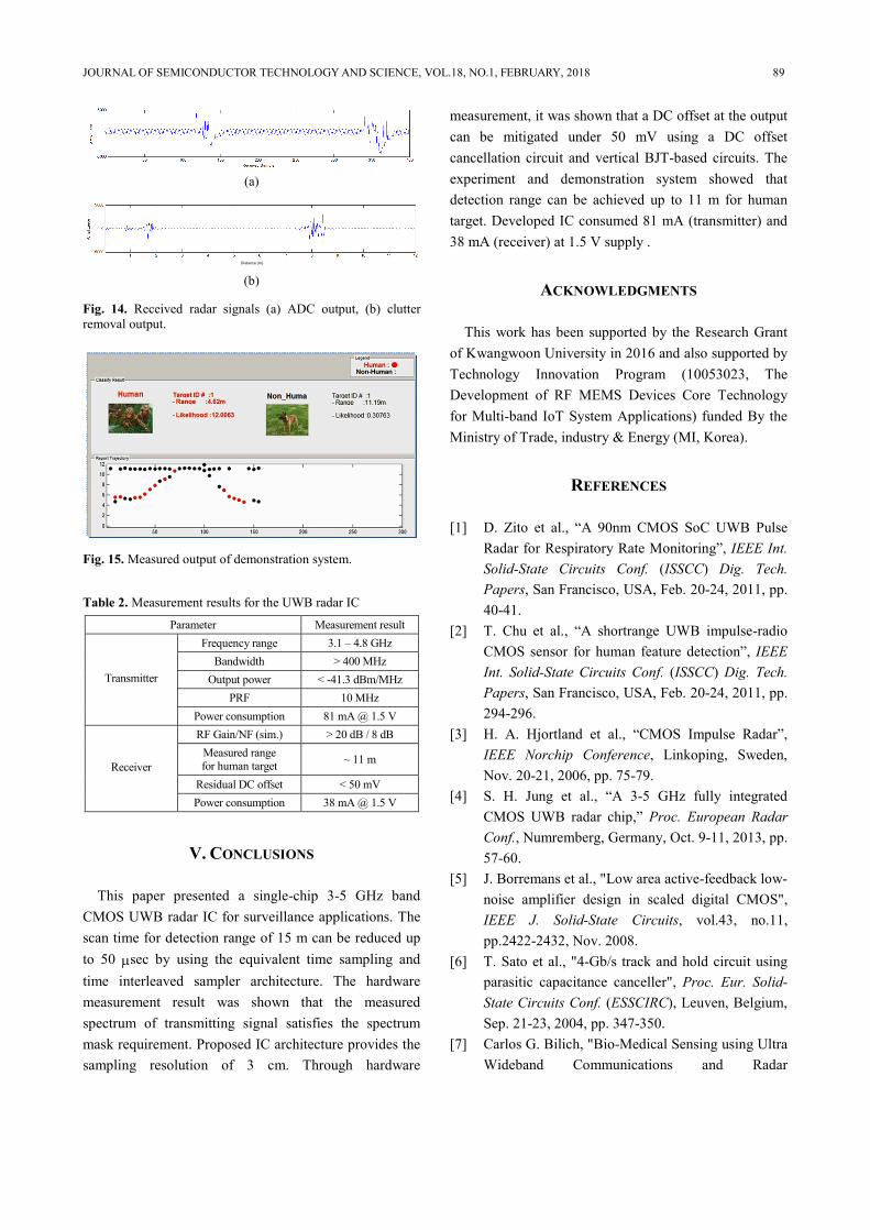
The impulse signal from UWB transmitter is passing through the cable and tunable RF attenuator, and finally enters into the receiver. Fig. 12 presents the measured receiver outputs with a cable length of 2.5 m and 4.5 m, respectively. Considering that cable length is 2 m long and dielectric constant of coaxial cable material is 2.1, the arrival time difference is approximately 9.6 ns. And the DC offset at the output can be mitigated under 50 mV.
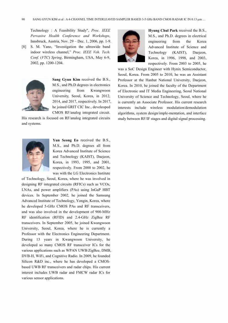
A digital signal processing (DSP) module is developed to measure the system-level performance of the proposed UWB radar IC. Fig. 13 presents a block diagram of the DSP module, which is implemented in an XC6SLX100
2 In [7], it was shown that the calculated path loss of radar is approximately 63 dB given a distance of 3 m, the projected area of the human body is approximately 900 cm2, and the reflection occurs primarily at the surface of the human skin. According to [7], a 60-dB attenuator is used for a total path loss of approximately 63 – 64 dB, and the gain of the directional antenna is assumed to be 10 dB. Each channel is equalized using VGA in the ASP block, and it is assumed that the DC offset is not changed during the short scanning time.
field-programmable gate array (FPGA). The resolution and sampling rate of the external analog-to-digital converter (ADC) are 8 bits and 10 ks/s, respectively. The received signal is matched filtered via cross-correlation with the reference pulse. In the clutter removal block, the CLEAN algorithm is used to suppress clutter [8]. And, the target is determined and classified using the likelihood calculator. Fig. 14 shows the ADC output signal and signal after clutter removal. Fig. 15 presents the final output of the system, which provides information about the distance and whether the target is human or animal. The radar module adds the external amplifiers both for Tx and Rx for raising the RF power and extending the detection range. As in Fig. 15, the distance and time are represented on the y-axis and x-axis, respectively, where a red circle indicates that when the target is human, the maximum measured range is 11 m. Conclusively, Table 2 summarizes the measure- ment results for the UWB radar IC.
Fig. 11. DC offset outputs before/after DC cancellation.
Fig. 12. Measured receiver outputs with a cable length of 2.5 m and 4.5 m.
UWBRadar
ICBPF
correlatorReference
pulse
Clutterremoval
Likelihoodcalculator
Fig. 13. Block diagram of DSP module.
JOURNAL OF SEMICONDUCTOR TECHNOLOGY AND SCIENCE, VOL.18, NO.1, FEBRUARY, 2018 89
V. CONCLUSIONS
This paper presented a single-chip 3-5 GHz band CMOS UWB radar IC for surveillance applications. The scan time for detection range of 15 m can be reduced up to 50 msec by using the equivalent time sampling and time interleaved sampler architecture. The hardware measurement result was shown that the measured spectrum of transmitting signal satisfies the spectrum mask requirement. Proposed IC architecture provides the sampling resolution of 3 cm. Through hardware
measurement, it was shown that a DC offset at the output can be mitigated under 50 mV using a DC offset cancellation circuit and vertical BJT-based circuits. The experiment and demonstration system showed that detection range can be achieved up to 11 m for human target. Developed IC consumed 81 mA (transmitter) and 38 mA (receiver) at 1.5 V supply .
ACKNOWLEDGMENTS
This work has been supported by the Research Grant of Kwangwoon University in 2016 and also supported by Technology Innovation Program (10053023, The Development of RF MEMS Devices Core Technology for Multi-band IoT System Applications) funded By the Ministry of Trade, industry & Energy (MI, Korea).
REFERENCES
[1] D. Zito et al., “A 90nm CMOS SoC UWB Pulse Radar for Respiratory Rate Monitoring”, IEEE Int. Solid-State Circuits Conf. (ISSCC) Dig. Tech. Papers, San Francisco, USA, Feb. 20-24, 2011, pp. 40-41.
[2] T. Chu et al., “A shortrange UWB impulse-radio CMOS sensor for human feature detection”, IEEE Int. Solid-State Circuits Conf. (ISSCC) Dig. Tech. Papers, San Francisco, USA, Feb. 20-24, 2011, pp. 294-296.
[3] H. A. Hjortland et al., “CMOS Impulse Radar”, IEEE Norchip Conference, Linkoping, Sweden, Nov. 20-21, 2006, pp. 75-79.
[4] S. H. Jung et al., “A 3-5 GHz fully integrated CMOS UWB radar chip,” Proc. European Radar Conf., Numremberg, Germany, Oct. 9-11, 2013, pp. 57-60.
[5] J. Borremans et al., "Low area active-feedback low-noise amplifier design in scaled digital CMOS", IEEE J. Solid-State Circuits, vol.43, no.11, pp.2422-2432, Nov. 2008.
[6] T. Sato et al., "4-Gb/s track and hold circuit using parasitic capacitance canceller", Proc. Eur. Solid-State Circuits Conf. (ESSCIRC), Leuven, Belgium, Sep. 21-23, 2004, pp. 347-350.
[7] Carlos G. Bilich, "Bio-Medical Sensing using Ultra Wideband Communications and Radar
(a)
Distance (m)
(b)
Fig. 14. Received radar signals (a) ADC output, (b) clutter removal output.
Fig. 15. Measured output of demonstration system.
Table 2. Measurement results for the UWB radar IC
Parameter Measurement result Frequency range 3.1 – 4.8 GHz
Bandwidth > 400 MHz Output power < -41.3 dBm/MHz
PRF 10 MHz
Transmitter
Power consumption 81 mA @ 1.5 V RF Gain/NF (sim.) > 20 dB / 8 dB
Measured range for human target ~ 11 m
Residual DC offset < 50 mV Receiver
Power consumption 38 mA @ 1.5 V
90 SANG GYUN KIM et al : A 4-CHANNEL TIME INTERLEAVED SAMPLER BASED 3-5 GHz BAND CMOS RADAR IC IN 0.13 mm …
Technology : A Feasibility Study", Proc. IEEE Pervasive Health Conference and Workshops, Innsbruck, Austria, Nov. 29 – Dec. 1, 2006, pp. 1-9.
[8] S. M. Yano, “Investigation the ultrawide band indoor wireless channel,” Proc. IEEE Veh. Tech. Conf. (VTC) Spring, Birmingham, USA, May 6-9, 2002, pp. 1200-1204.
Sang Gyun Kim received the B.S., M.S., and Ph.D degrees in electronics engineering from Kwangwoon University, Seoul, Korea, in 2012, 2014, and 2017, respectively. In 2017, he joined GRIT CIC Inc., develeoped CMOS RF/analog integrated circuit.
His research is focused on RF/analog integrated circuits and systems.
Yun Seong Eo received the B.S., M.S., and Ph.D. degrees all from Korea Advanced Institute of Science and Technology (KAIST), Daejeon, Korea, in 1993, 1995, and 2001, respectively. From 2000 to 2002, he was with the LG Electronics Institute
of Technology, Seoul, Korea, where he was involved in designing RF integrated circuits (RFICs) such as VCOs, LNAs, and power amplifiers (PAs) using InGaP HBT devices. In September 2002, he joined the Samsung Advanced Institute of Technology, Yongin, Korea, where he developed 5-GHz CMOS PAs and RF transceivers, and was also involved in the development of 900-MHz RF identification (RFID) and 2.4-GHz ZigBee RF transceivers. In September 2005, he joined Kwangwoon University, Seoul, Korea, where he is currently a Professor with the Electronics Engineering Department. During 13 years in Kwangwoon University, he developed so many CMOS RF transceiver ICs for the various applications such as WPAN UWB/ZigBee, DMB, DVB-H, WiFi, and Cognitive Radio. In 2009, he founded Silicon R&D inc., where he has developed a CMOS-based UWB RF transceivers and radar chips. His current interest includes UWB radar and FMCW radar ICs for various sensor applications.
Hyung Chul Park received the B.S., M.S., and Ph.D. degrees in electrical engineering from the Korea Advanced Institute of Science and Technology (KAIST), Daejeon, Korea, in 1996, 1998, and 2003, respectively. From 2003 to 2005, he
was a SoC Design Engineer with Hynix Semiconductor, Seoul, Korea. From 2005 to 2010, he was an Assistant Professor at the Hanbat National University, Daejeon, Korea. In 2010, he joined the faculty of the Department of Electronic and IT Media Engineering, Seoul National University of Science and Technology, Seoul, where he is currently an Associate Professor. His current research interests include wireless modulation/demodulation algorithms, system design/imple-mentation, and interface study between RF/IF stages and digital signal processing.