802.15.3c
TRANSCRIPT
Institutionen för systemteknikDepartment of Electrical Engineering
Examensarbete
High Level Model of IEEE 802.15.3c Standard andImplementation of a Suitable FFT on ASIC
Examensarbete utfört i Elektroniksystemvid Tekniska högskolan vid Linköpings universitet
av
Tanvir Ahmed
LiTH-ISY-EX--11/4462--SE
Linköping 2011
Department of Electrical Engineering Linköpings tekniska högskolaLinköpings universitet Linköpings universitetSE-581 83 Linköping, Sweden 581 83 Linköping

High Level Model of IEEE 802.15.3c Standard andImplementation of a Suitable FFT on ASIC
Examensarbete utfört i Elektroniksystemvid Tekniska högskolan i Linköping
av
Tanvir Ahmed
LiTH-ISY-EX--11/4462--SE
Handledare: Carl Ingemarssonisy, Linköpings universitet
Mario Garridoisy, Linköings universitet
Examinator: Oscar Gustafssonisy, Linköpings universitet
Linköping, 15 May, 2011

Avdelning, InstitutionDivision, Department
Electronics SystemsDepartment of Electrical EngineeringLinköpings universitetSE-581 83 Linköping, Sweden
DatumDate
2011-05-15
SpråkLanguage
� Svenska/Swedish
� Engelska/English
�
�
RapporttypReport category
� Licentiatavhandling
� Examensarbete
� C-uppsats
� D-uppsats
� Övrig rapport
�
�
URL för elektronisk versionhttp://www.es.isy.liu.se
http://urn.kb.se/resolve?urn=urn:nbn:se:liu:diva-68697
ISBN
—
ISRN
LiTH-ISY-EX--11/4462--SE
Serietitel och serienummerTitle of series, numbering
ISSN
—
TitelTitle
Svensk titelHigh Level Model of IEEE 802.15.3c Standard and Implementation of a SuitableFFT on ASIC
FörfattareAuthor
Tanvir Ahmed
SammanfattningAbstract
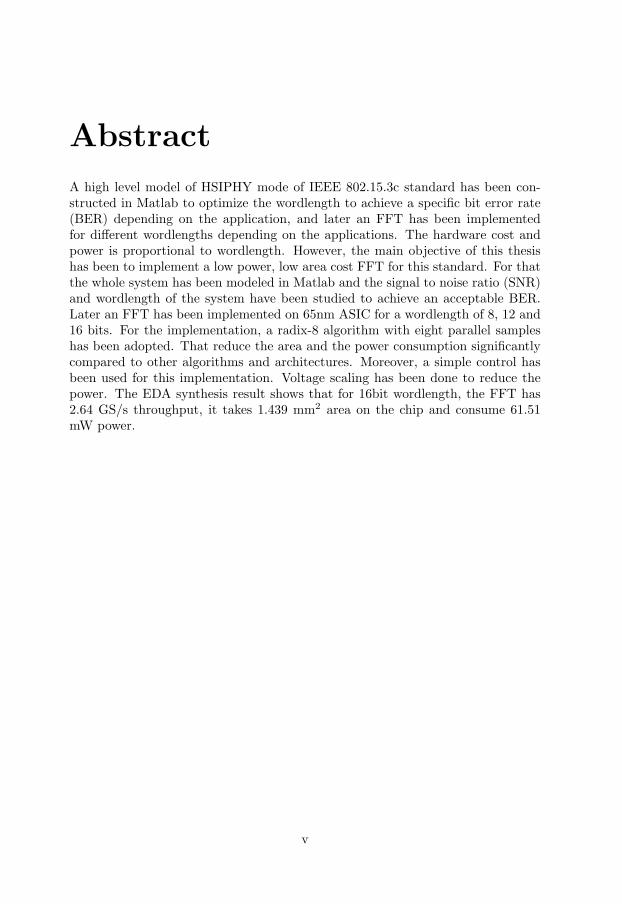
A high level model of HSIPHY mode of IEEE 802.15.3c standard has been con-structed in Matlab to optimize the wordlength to achieve a specific bit error rate(BER) depending on the application, and later an FFT has been implementedfor different wordlengths depending on the applications. The hardware cost andpower is proportional to wordlength. However, the main objective of this thesishas been to implement a low power, low area cost FFT for this standard. For thatthe whole system has been modeled in Matlab and the signal to noise ratio (SNR)and wordlength of the system have been studied to achieve an acceptable BER.Later an FFT has been implemented on 65nm ASIC for a wordlength of 8, 12 and16 bits. For the implementation, a radix-8 algorithm with eight parallel sampleshas been adopted. That reduce the area and the power consumption significantlycompared to other algorithms and architectures. Moreover, a simple control hasbeen used for this implementation. Voltage scaling has been done to reduce thepower. The EDA synthesis result shows that for 16bit wordlength, the FFT has2.64 GS/s throughput, it takes 1.439 mm2 area on the chip and consume 61.51mW power.
NyckelordKeywords WPAN, FFT, ASIC, Radix-8

AbstractA high level model of HSIPHY mode of IEEE 802.15.3c standard has been con-structed in Matlab to optimize the wordlength to achieve a specific bit error rate(BER) depending on the application, and later an FFT has been implementedfor different wordlengths depending on the applications. The hardware cost andpower is proportional to wordlength. However, the main objective of this thesishas been to implement a low power, low area cost FFT for this standard. For thatthe whole system has been modeled in Matlab and the signal to noise ratio (SNR)and wordlength of the system have been studied to achieve an acceptable BER.Later an FFT has been implemented on 65nm ASIC for a wordlength of 8, 12 and16 bits. For the implementation, a radix-8 algorithm with eight parallel sampleshas been adopted. That reduce the area and the power consumption significantlycompared to other algorithms and architectures. Moreover, a simple control hasbeen used for this implementation. Voltage scaling has been done to reduce thepower. The EDA synthesis result shows that for 16bit wordlength, the FFT has2.64 GS/s throughput, it takes 1.439 mm2 area on the chip and consume 61.51mW power.
v


Acknowledgments
I would like to thank Oscar Gustafsson for giving me an opportunity to do mythesis in Electronics Systems. That gives me the access of the resources and allkind of facilities for doing my thesis. It gives me a new way of thinking and Ibelieve that it will help me for my PhD in Japan. I am heartily thankful to mysupervisors Carl Ingemarsson and Mario Garrido for guiding throughout the thesisand correcting various documents of mine with attention and care. Apart fromthat they helped me a lot to solve the technical issues related with the thesis.Their guidance helped me to get a grip on different design tool and VHDL, suchthat Matlab, Modelsim and Design Compiler. I offer my regards and blessing to allmy friends who were sharing the lab with me for their inspiration and exchangingtheir culture and ideas. It was a great experience for me to work with differentpeople from different countries and experiencing the multicultural environment.As well as it helps me a lot to know about different areas of electronics as theywere working in different topics.
Last but not least I am grateful to my parents for giving me every kind ofsupport from my birth untill now. I believe that without their support it was notpossible for me to continuing my Master’s in Sweden.
vii

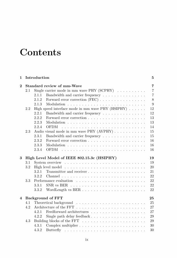
Contents
1 Introduction 5
2 Standard review of mm-Wave 72.1 Single carrier mode in mm wave PHY (SCPHY) . . . . . . . . . . 7
2.1.1 Bandwidth and carrier frequency . . . . . . . . . . . . . . . 72.1.2 Forward error correction (FEC) . . . . . . . . . . . . . . . . 82.1.3 Modulation . . . . . . . . . . . . . . . . . . . . . . . . . . . 9
2.2 High speed interface mode in mm wave PHY (HSIPHY) . . . . . . 122.2.1 Bandwidth and carrier frequency . . . . . . . . . . . . . . . 122.2.2 Forward error correction . . . . . . . . . . . . . . . . . . . . 132.2.3 Modulation . . . . . . . . . . . . . . . . . . . . . . . . . . . 132.2.4 OFDM . . . . . . . . . . . . . . . . . . . . . . . . . . . . . 14
2.3 Audio visual mode in mm wave PHY (AVPHY) . . . . . . . . . . . 152.3.1 Bandwidth and carrier frequency . . . . . . . . . . . . . . . 152.3.2 Forward error correction . . . . . . . . . . . . . . . . . . . . 162.3.3 Modulation . . . . . . . . . . . . . . . . . . . . . . . . . . . 162.3.4 OFDM . . . . . . . . . . . . . . . . . . . . . . . . . . . . . 16
3 High Level Model of IEEE 802.15.3c (HSIPHY) 193.1 System overview . . . . . . . . . . . . . . . . . . . . . . . . . . . . 193.2 High level model . . . . . . . . . . . . . . . . . . . . . . . . . . . . 20
3.2.1 Transmitter and receiver . . . . . . . . . . . . . . . . . . . . 213.2.2 Channel . . . . . . . . . . . . . . . . . . . . . . . . . . . . . 22
3.3 Performance evaluation . . . . . . . . . . . . . . . . . . . . . . . . 223.3.1 SNR vs BER . . . . . . . . . . . . . . . . . . . . . . . . . . 223.3.2 WordLength vs BER . . . . . . . . . . . . . . . . . . . . . . 22
4 Background of FFT 254.1 Theoretical background . . . . . . . . . . . . . . . . . . . . . . . . 254.2 Architecture of the FFT . . . . . . . . . . . . . . . . . . . . . . . . 27
4.2.1 Feedforward architectures . . . . . . . . . . . . . . . . . . . 274.2.2 Single path delay feedback . . . . . . . . . . . . . . . . . . . 29
4.3 Building blocks of the FFT . . . . . . . . . . . . . . . . . . . . . . 294.3.1 Complex multiplier . . . . . . . . . . . . . . . . . . . . . . . 304.3.2 Butterfly . . . . . . . . . . . . . . . . . . . . . . . . . . . . 30
ix
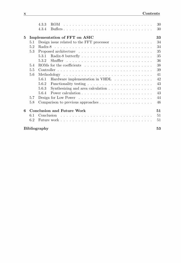
x Contents
4.3.3 ROM . . . . . . . . . . . . . . . . . . . . . . . . . . . . . . 304.3.4 Buffers . . . . . . . . . . . . . . . . . . . . . . . . . . . . . . 30
5 Implementation of FFT on ASIC 335.1 Design issue related to the FFT processor . . . . . . . . . . . . . . 345.2 Radix-8 . . . . . . . . . . . . . . . . . . . . . . . . . . . . . . . . . 345.3 Proposed architecture . . . . . . . . . . . . . . . . . . . . . . . . . 35
5.3.1 Radix-8 butterfly . . . . . . . . . . . . . . . . . . . . . . . . 355.3.2 Shuffler . . . . . . . . . . . . . . . . . . . . . . . . . . . . . 36
5.4 ROMs for the coefficients . . . . . . . . . . . . . . . . . . . . . . . 385.5 Controller . . . . . . . . . . . . . . . . . . . . . . . . . . . . . . . . 395.6 Methodology . . . . . . . . . . . . . . . . . . . . . . . . . . . . . . 41
5.6.1 Hardware implementation in VHDL . . . . . . . . . . . . . 425.6.2 Functionality testing . . . . . . . . . . . . . . . . . . . . . . 435.6.3 Synthesizing and area calculation . . . . . . . . . . . . . . . 435.6.4 Power calculation . . . . . . . . . . . . . . . . . . . . . . . . 43
5.7 Design for Low Power . . . . . . . . . . . . . . . . . . . . . . . . . 445.8 Comparison to previous approaches . . . . . . . . . . . . . . . . . . 46
6 Conclusion and Future Work 516.1 Conclusion . . . . . . . . . . . . . . . . . . . . . . . . . . . . . . . 516.2 Future work . . . . . . . . . . . . . . . . . . . . . . . . . . . . . . . 51
Bibliography 53
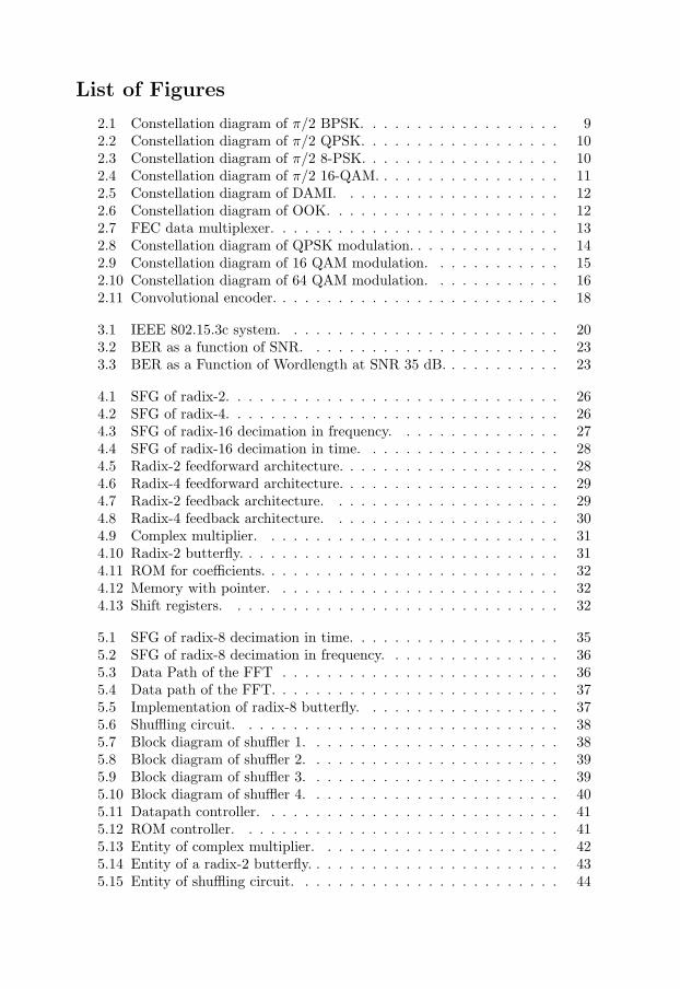
List of Figures2.1 Constellation diagram of π/2 BPSK. . . . . . . . . . . . . . . . . . 92.2 Constellation diagram of π/2 QPSK. . . . . . . . . . . . . . . . . . 102.3 Constellation diagram of π/2 8-PSK. . . . . . . . . . . . . . . . . . 102.4 Constellation diagram of π/2 16-QAM. . . . . . . . . . . . . . . . . 112.5 Constellation diagram of DAMI. . . . . . . . . . . . . . . . . . . . 122.6 Constellation diagram of OOK. . . . . . . . . . . . . . . . . . . . . 122.7 FEC data multiplexer. . . . . . . . . . . . . . . . . . . . . . . . . . 132.8 Constellation diagram of QPSK modulation. . . . . . . . . . . . . . 142.9 Constellation diagram of 16 QAM modulation. . . . . . . . . . . . 152.10 Constellation diagram of 64 QAM modulation. . . . . . . . . . . . 162.11 Convolutional encoder. . . . . . . . . . . . . . . . . . . . . . . . . . 18
3.1 IEEE 802.15.3c system. . . . . . . . . . . . . . . . . . . . . . . . . 203.2 BER as a function of SNR. . . . . . . . . . . . . . . . . . . . . . . 233.3 BER as a Function of Wordlength at SNR 35 dB. . . . . . . . . . . 23
4.1 SFG of radix-2. . . . . . . . . . . . . . . . . . . . . . . . . . . . . . 264.2 SFG of radix-4. . . . . . . . . . . . . . . . . . . . . . . . . . . . . . 264.3 SFG of radix-16 decimation in frequency. . . . . . . . . . . . . . . 274.4 SFG of radix-16 decimation in time. . . . . . . . . . . . . . . . . . 284.5 Radix-2 feedforward architecture. . . . . . . . . . . . . . . . . . . . 284.6 Radix-4 feedforward architecture. . . . . . . . . . . . . . . . . . . . 294.7 Radix-2 feedback architecture. . . . . . . . . . . . . . . . . . . . . 294.8 Radix-4 feedback architecture. . . . . . . . . . . . . . . . . . . . . 304.9 Complex multiplier. . . . . . . . . . . . . . . . . . . . . . . . . . . 314.10 Radix-2 butterfly. . . . . . . . . . . . . . . . . . . . . . . . . . . . . 314.11 ROM for coefficients. . . . . . . . . . . . . . . . . . . . . . . . . . . 324.12 Memory with pointer. . . . . . . . . . . . . . . . . . . . . . . . . . 324.13 Shift registers. . . . . . . . . . . . . . . . . . . . . . . . . . . . . . 32
5.1 SFG of radix-8 decimation in time. . . . . . . . . . . . . . . . . . . 355.2 SFG of radix-8 decimation in frequency. . . . . . . . . . . . . . . . 365.3 Data Path of the FFT . . . . . . . . . . . . . . . . . . . . . . . . . 365.4 Data path of the FFT. . . . . . . . . . . . . . . . . . . . . . . . . . 375.5 Implementation of radix-8 butterfly. . . . . . . . . . . . . . . . . . 375.6 Shuffling circuit. . . . . . . . . . . . . . . . . . . . . . . . . . . . . 385.7 Block diagram of shuffler 1. . . . . . . . . . . . . . . . . . . . . . . 385.8 Block diagram of shuffler 2. . . . . . . . . . . . . . . . . . . . . . . 395.9 Block diagram of shuffler 3. . . . . . . . . . . . . . . . . . . . . . . 395.10 Block diagram of shuffler 4. . . . . . . . . . . . . . . . . . . . . . . 405.11 Datapath controller. . . . . . . . . . . . . . . . . . . . . . . . . . . 415.12 ROM controller. . . . . . . . . . . . . . . . . . . . . . . . . . . . . 415.13 Entity of complex multiplier. . . . . . . . . . . . . . . . . . . . . . 425.14 Entity of a radix-2 butterfly. . . . . . . . . . . . . . . . . . . . . . . 435.15 Entity of shuffling circuit. . . . . . . . . . . . . . . . . . . . . . . . 44

2 Contents
5.16 Area and power consumption of the FFT before and after frequencyscaling. . . . . . . . . . . . . . . . . . . . . . . . . . . . . . . . . . 45
5.17 Power consumption before and after voltage scaling. . . . . . . . . 455.18 Power and area for different length buffer. . . . . . . . . . . . . . . 465.19 Power and area of complex multiplier. . . . . . . . . . . . . . . . . 475.20 Power and area of radix-8 butterfly. . . . . . . . . . . . . . . . . . 485.21 Power and area of FFT. . . . . . . . . . . . . . . . . . . . . . . . . 49
Contents 3
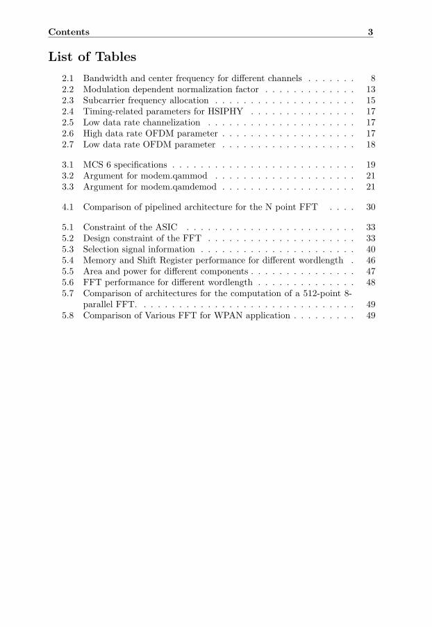
List of Tables2.1 Bandwidth and center frequency for different channels . . . . . . . 82.2 Modulation dependent normalization factor . . . . . . . . . . . . . 132.3 Subcarrier frequency allocation . . . . . . . . . . . . . . . . . . . . 152.4 Timing-related parameters for HSIPHY . . . . . . . . . . . . . . . 172.5 Low data rate channelization . . . . . . . . . . . . . . . . . . . . . 172.6 High data rate OFDM parameter . . . . . . . . . . . . . . . . . . . 172.7 Low data rate OFDM parameter . . . . . . . . . . . . . . . . . . . 18
3.1 MCS 6 specifications . . . . . . . . . . . . . . . . . . . . . . . . . . 193.2 Argument for modem.qammod . . . . . . . . . . . . . . . . . . . . 213.3 Argument for modem.qamdemod . . . . . . . . . . . . . . . . . . . 21
4.1 Comparison of pipelined architecture for the N point FFT . . . . 30
5.1 Constraint of the ASIC . . . . . . . . . . . . . . . . . . . . . . . . 335.2 Design constraint of the FFT . . . . . . . . . . . . . . . . . . . . . 335.3 Selection signal information . . . . . . . . . . . . . . . . . . . . . . 405.4 Memory and Shift Register performance for different wordlength . 465.5 Area and power for different components . . . . . . . . . . . . . . . 475.6 FFT performance for different wordlength . . . . . . . . . . . . . . 485.7 Comparison of architectures for the computation of a 512-point 8-
parallel FFT. . . . . . . . . . . . . . . . . . . . . . . . . . . . . . . 495.8 Comparison of Various FFT for WPAN application . . . . . . . . . 49

Chapter 1
Introduction
The advancement of the applications in communication systems as well as thedata rate of the applications are racing with time. Different task groups developeddifferent standards and some of them are adopted by the IEEE. IEEE 802.15.3cis one of them. Some other applications of IEEE 802.15 standard are Bluetoothand Zigbee. These standards can support a data rate up to 100 Mb/s for shortrange (1 m - 10 m) communication. However, those atandards are not suitable forapplications such as Live HD video streaming with a bit rate ∼3 Gbps, to replacethe HDMI (2.2 Gbps) connection with wireless connectivity and large file transferat very high speed.
In 2005, IEEE 802.15 Alternative Task Group 3c developed a standard withan aim of providing wireless communication in a person’s area while the data ratewill be high enough to support those applications [1]. This standard uses the 60GHz band as a carrier frequency. However, research shows that the band near 60GHz has high attenuation in air compared to the 5 GHz band. As aresult, thisband is more suitable for indoor rather than outdoor applictions. Moreover, itcan limit the problem of channel interference. Later, in 2009, the standard wasadopted by IEEE.
The title of the thesis work is “High Level Model of IEEE 802.15.3c and Im-plementation of a Suitable FFT on ASIC” There are two components to this title.The first one, high level model of the IEEE 802.15.3c standard. That includethe exploration of the different aspects of the standard. Such as, Review of thestandard and a high level model of one specific mode for this standard. The highlevel model has been used to optimized the different parameter (such as SNR andfinite word length) for the physical layer. Second component is the implementationof a suitable FFT on ASIC. HSIPHY mode of this standard adopted orthogonalfrequency division multiplexing (OFDM) to overcome multipath fading effect ofwireless channel and FFT is the key component of OFDM. To implement an FFTon ASIC, a 65 nm technology standard cell library has been used. The mainattention of the implementation was to reduce the power as well as the area.
This document is organized in the following chapters:
• Chapter 1: Introduction
5
6 Introduction
• Chapter 2: Standard Review of mm-Wave- A review of the IEEE 802.15.3cstandard and its different mode of operations.
• Chapter 3: High Level Model of IEEE 802.15.3c (HSIPHY) - Modelingof physical layer for High Speed Interface (HSIPHY) and effect of finitewordlength and SNR on bit error rate.
• Chapter 4: Backround of the FFT - Discussion about the algorithm of thediscrete Fourier transform (DFT), different architectures of the FFT and thebasic building blocks.
• Chapter 5: Implementation of the FFT on ASIC - Details of radix-8 anddesign issue, hardware implementation and results of the FFT.
• Chapter 6: Conclusion and Future Work - Different conclusions are drawnon the basis of the results and some direction for the research.
The whole design is based on Matlab and VHDL. Communication toolbox ofMatlab has been used for the high level model of the standard and VHDL asa hardware description language for the implementation of the FFT. Modelsimand Design compiler have been used for the functionality testing and compilationof the design for a specific technology library, respectively. Finally, performancemeasurement (calculation of the power and area for a specific clock frequency) hasbeen done by means of Design compiler and Nanosim.
Chapter 2
Standard review ofmm-Wave
This chapter focuses on the standard review of the IEEE 802.15.3c. This standardis mostly used for high data rate transmission at GBPS rates such as video ondemand, HDTV and home theater and data transmission at Gbps data rate. Thisstandard use 60GHz as a carrier frequency [1]. This band a high attenuation infree space. Research shows that the 60 GHz band has attenuation of 15 dB perkilometer. So, this band is a promising candidate for indoor applications ratherthan outdoor.
It is noted in [1] that the standard can operate in three different mode.
• Single Carrier mode in mmWave PHY (SCPHY)
• High Speed Interface mode in mmWave PHY (HSIPHY)
• Audio/Visual mode in mmWave PHY (AVPHY)
2.1 Single carrier mode in mm wave PHY (SC-PHY)
This mode provides three different classes of modulation and coding scheme tar-geting different wireless connectivity applications. Class 1 has been specified forlow rate and low cost mobile operation while this mode can support a data rate1.5 Gb/s. Class 2 has been specified to achieve a data rate up to 3 Gb/s and class3 has been specified for the high speed and high performance applications with adata rate over 5 Gb/s [1].
2.1.1 Bandwidth and carrier frequencyThis mode operates in four different carrier frequency that ranges between 57.24GHz to 65.88 GHz [1]. However the bandwidth remains equal for all four cases.These channels are defined in Table 2.1.
7
8 Standard review of mm-Wave
Table 2.1: Bandwidth and center frequency for different channelsChannel ID Start frequency Center frequency Stop frequency
1 57.24 58.32 59.402 59.40 60.48 61.563 61.56 62.64 63.724 63.72 64.80 65.88
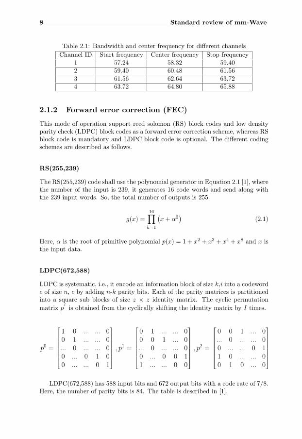
2.1.2 Forward error correction (FEC)
This mode of operation support reed solomon (RS) block codes and low densityparity check (LDPC) block codes as a forward error correction scheme, whereas RSblock code is mandatory and LDPC block code is optional. The different codingschemes are described as follows.
RS(255,239)
The RS(255,239) code shall use the polynomial generator in Equation 2.1 [1], wherethe number of the input is 239, it generates 16 code words and send along withthe 239 input words. So, the total number of outputs is 255.
g(x) =16∏
k=1
(x + α2
)(2.1)
Here, α is the root of primitive polynomial p(x) = 1 + x2 + x3 + x4 + x8 and x isthe input data.
LDPC(672,588)
LDPC is systematic, i.e., it encode an information block of size k,i into a codewordc of size n, c by adding n-k parity bits. Each of the parity matrices is partitionedinto a square sub blocks of size z × z identity matrix. The cyclic permutationmatrix p
I
is obtained from the cyclically shifting the identity matrix by I times.
p0 =
1 0 ... ... 00 1 ... ... 0... 0 ... ... 00 ... 0 1 00 ... ... 0 1
, p1 =
0 1 ... ... 00 0 1 ... 0... 0 ... ... 00 ... 0 0 11 ... ... 0 0
, p2 =
0 0 1 ... 0... 0 ... ... 00 ... ... 0 11 0 ... ... 00 1 0 ... 0
LDPC(672,588) has 588 input bits and 672 output bits with a code rate of 7/8.
Here, the number of parity bits is 84. The table is described in [1].
2.1 Single carrier mode in mm wave PHY (SCPHY) 9
LDPC(672,504)
There has 504 input bits and 672 output bit in LDPC(672,504) with a code rateof 3/4. The number of parity bits is 168. However, it follows the same identityand permuted matrix as discussed in Section 2.1.2. The table is described in [1]
LDPC(672,336)
LDPC(672,336) is used for highly reliable applications with a code rate of 1/2. Ittakes 336 bits as an input and generates 672 bits. It follows the identity matrix ofSection 2.1.2 and the table is described in [1].
2.1.3 ModulationThis mode supports six different modulation schemes depending on the data rateand the performance requirements of the applications. However, four of them aremandatory and the other two are optional. The optional schemes are used for lowdata rate application.
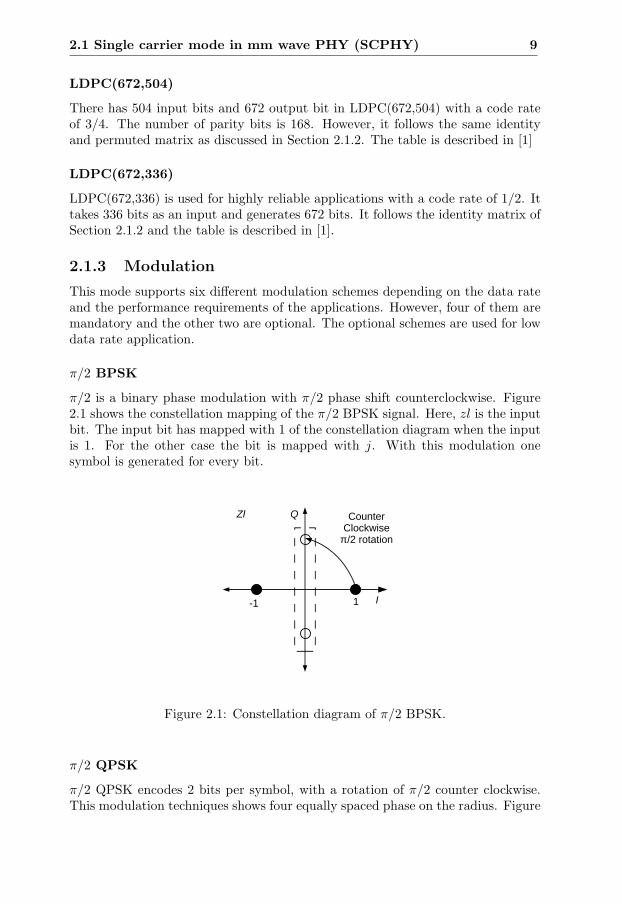
π/2 BPSK
π/2 is a binary phase modulation with π/2 phase shift counterclockwise. Figure2.1 shows the constellation mapping of the π/2 BPSK signal. Here, zl is the inputbit. The input bit has mapped with 1 of the constellation diagram when the inputis 1. For the other case the bit is mapped with j. With this modulation onesymbol is generated for every bit.
I
QZl
-1 1
CounterClockwise
π/2 rotation
Figure 2.1: Constellation diagram of π/2 BPSK.
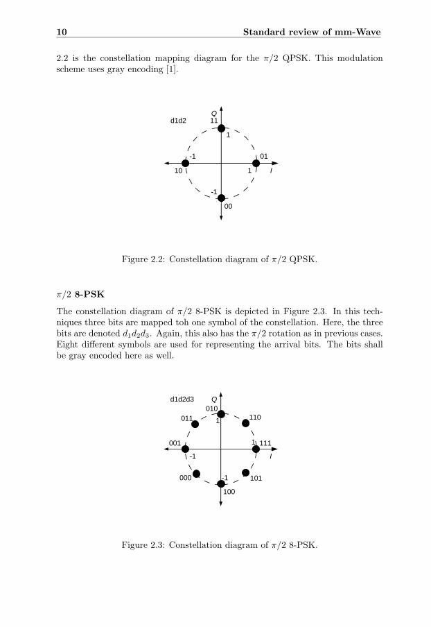
π/2 QPSK
π/2 QPSK encodes 2 bits per symbol, with a rotation of π/2 counter clockwise.This modulation techniques shows four equally spaced phase on the radius. Figure
10 Standard review of mm-Wave
2.2 is the constellation mapping diagram for the π/2 QPSK. This modulationscheme uses gray encoding [1].
I
Q11
01
10
00
d1d2
1
-1
-1
1
Figure 2.2: Constellation diagram of π/2 QPSK.
π/2 8-PSK
The constellation diagram of π/2 8-PSK is depicted in Figure 2.3. In this tech-niques three bits are mapped toh one symbol of the constellation. Here, the threebits are denoted d1d2d3. Again, this also has the π/2 rotation as in previous cases.Eight different symbols are used for representing the arrival bits. The bits shallbe gray encoded here as well.
1
1
-1
-1
I
Qd1d2d3
011
100
101000
001
010110
111
Figure 2.3: Constellation diagram of π/2 8-PSK.
2.1 Single carrier mode in mm wave PHY (SCPHY) 11
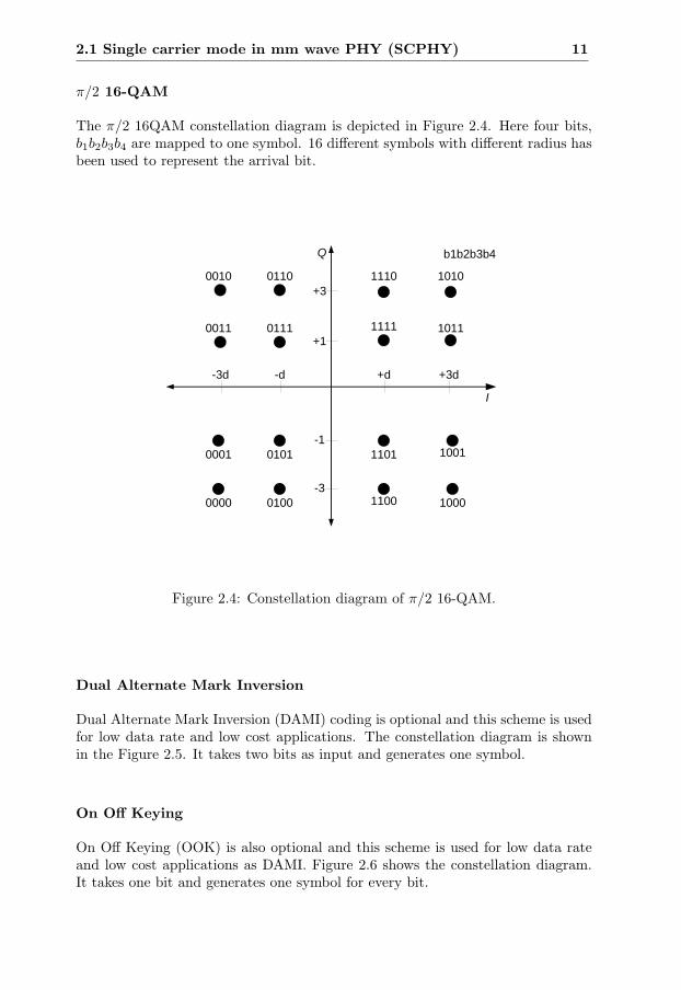
π/2 16-QAM
The π/2 16QAM constellation diagram is depicted in Figure 2.4. Here four bits,b1b2b3b4 are mapped to one symbol. 16 different symbols with different radius hasbeen used to represent the arrival bit.
I
+1
-d
-1
+d
b1b2b3b4Q
-3
+3
-3d +3d
0010 0110 1110 1010
0011 0111 1111 1011
0001
0000
0101
0100
1101
1100 1000
1001
Figure 2.4: Constellation diagram of π/2 16-QAM.
Dual Alternate Mark Inversion
Dual Alternate Mark Inversion (DAMI) coding is optional and this scheme is usedfor low data rate and low cost applications. The constellation diagram is shownin the Figure 2.5. It takes two bits as input and generates one symbol.
On Off Keying
On Off Keying (OOK) is also optional and this scheme is used for low data rateand low cost applications as DAMI. Figure 2.6 shows the constellation diagram.It takes one bit and generates one symbol for every bit.
12 Standard review of mm-Wave
Q
I11 1
10 011100
Figure 2.5: Constellation diagram of DAMI.
I
Q
10
Figure 2.6: Constellation diagram of OOK.
2.2 High speed interface mode in mm wave PHY(HSIPHY)
The HSI PHY is designed for low latency, high speed data and it use orthogonalfrequency domain multiplexing (OFDM). This mode supports different modulationand coding scheme using different frequency domain spreading factors, modula-tions and LDPC block codes.
2.2.1 Bandwidth and carrier frequency
This mode uses Channel IDs 2 and 3 of Table 2.1 as a carrier frequency [1]. Theband starts from 59.40 GHz and ends at 63.72 GHz. The center frequencies are60.48GHz and 62.64GHz respectively for Channel IDs 2 and 3.
2.2 High speed interface mode in mm wave PHY (HSIPHY) 13
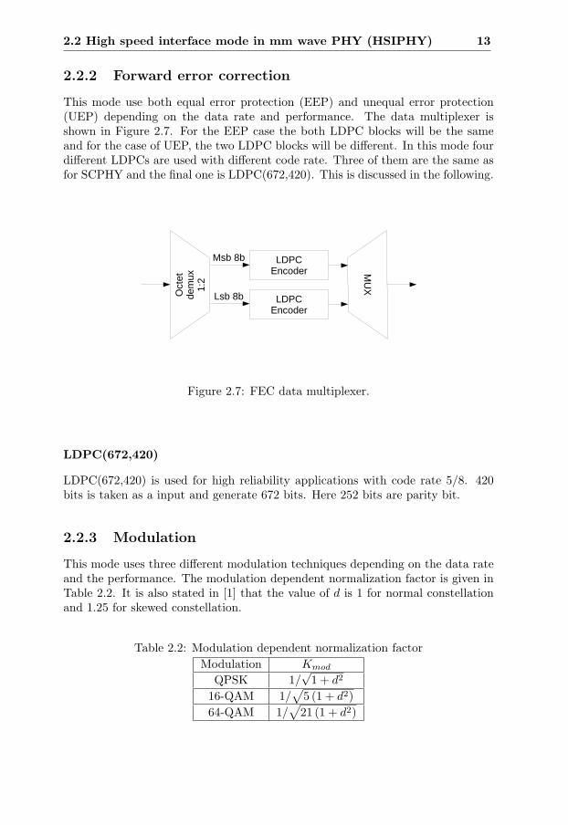
2.2.2 Forward error correction
This mode use both equal error protection (EEP) and unequal error protection(UEP) depending on the data rate and performance. The data multiplexer isshown in Figure 2.7. For the EEP case the both LDPC blocks will be the sameand for the case of UEP, the two LDPC blocks will be different. In this mode fourdifferent LDPCs are used with different code rate. Three of them are the same asfor SCPHY and the final one is LDPC(672,420). This is discussed in the following.
Oct
etde
mux
1:2
MU
X
LDPCEncoder
LDPCEncoder
Msb 8b
Lsb 8b
Figure 2.7: FEC data multiplexer.
LDPC(672,420)
LDPC(672,420) is used for high reliability applications with code rate 5/8. 420bits is taken as a input and generate 672 bits. Here 252 bits are parity bit.
2.2.3 Modulation
This mode uses three different modulation techniques depending on the data rateand the performance. The modulation dependent normalization factor is given inTable 2.2. It is also stated in [1] that the value of d is 1 for normal constellationand 1.25 for skewed constellation.
Table 2.2: Modulation dependent normalization factorModulation Kmod
QPSK 1/√
1 + d2
16-QAM 1/√
5 (1 + d2)64-QAM 1/
√21 (1 + d2)
14 Standard review of mm-Wave
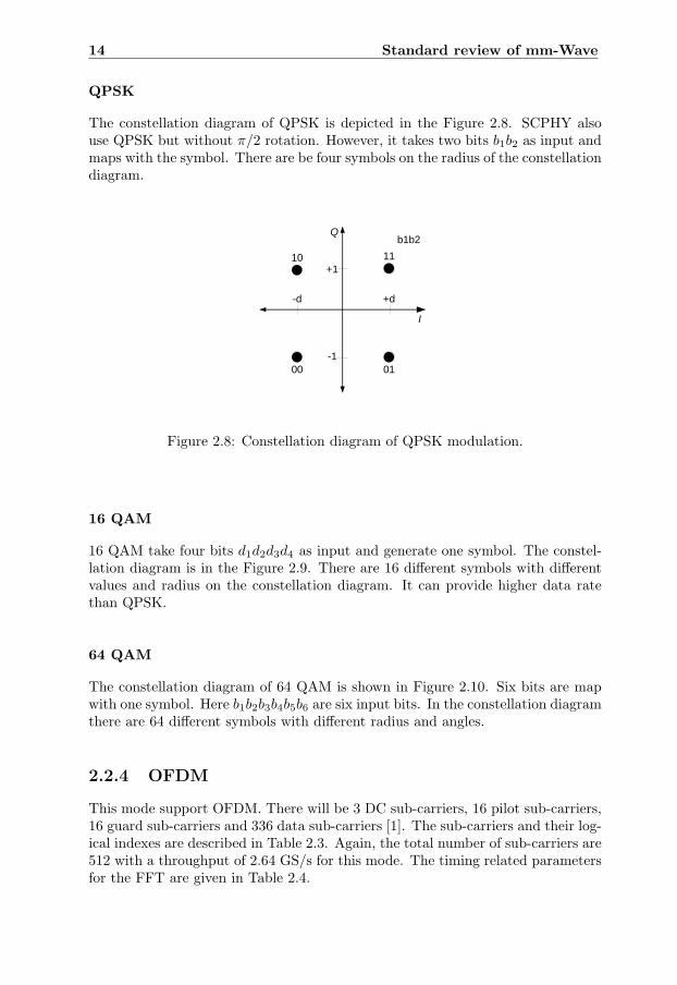
QPSK
The constellation diagram of QPSK is depicted in the Figure 2.8. SCPHY alsouse QPSK but without π/2 rotation. However, it takes two bits b1b2 as input andmaps with the symbol. There are be four symbols on the radius of the constellationdiagram.
I
Q
+1
-d
-1
+d
10 11
0100
b1b2
Figure 2.8: Constellation diagram of QPSK modulation.
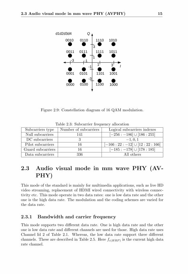
16 QAM
16 QAM take four bits d1d2d3d4 as input and generate one symbol. The constel-lation diagram is in the Figure 2.9. There are 16 different symbols with differentvalues and radius on the constellation diagram. It can provide higher data ratethan QPSK.
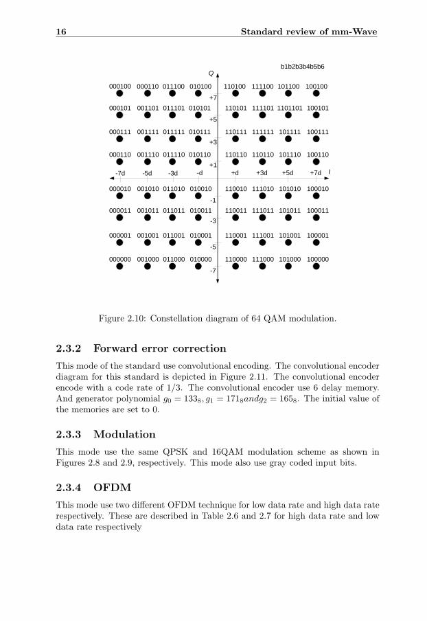
64 QAM
The constellation diagram of 64 QAM is shown in Figure 2.10. Six bits are mapwith one symbol. Here b1b2b3b4b5b6 are six input bits. In the constellation diagramthere are 64 different symbols with different radius and angles.
2.2.4 OFDM
This mode support OFDM. There will be 3 DC sub-carriers, 16 pilot sub-carriers,16 guard sub-carriers and 336 data sub-carriers [1]. The sub-carriers and their log-ical indexes are described in Table 2.3. Again, the total number of sub-carriers are512 with a throughput of 2.64 GS/s for this mode. The timing related parametersfor the FFT are given in Table 2.4.
2.3 Audio visual mode in mm wave PHY (AVPHY) 15
Q
I
d1d2d3d4
0000
0001
0010
0011
0100
0101
0110
0111
1000
1001
1010
1011
1101
1110
1100
1111
1
1-1
-1
3
3-3
-3
Figure 2.9: Constellation diagram of 16 QAM modulation.
Table 2.3: Subcarrier frequency allocationSubcarriers type Number of subcarriers Logical subcarriers indexesNull subcarriers 141 [−256 : −186] ∪ [186 : 255]DC subcarriers 3 −1, 0, 1
Pilot subcarriers 16 [−166 : 22 : −12] ∪ [12 : 22 : 166]Guard subcarriers 16 [−185 : −178] ∪ [178 : 185]Data subcarriers 336 All others
2.3 Audio visual mode in mm wave PHY (AV-PHY)
This mode of the standard is mainly for multimedia applications, such as live HDvideo streaming, replacement of HDMI wired connectivity with wireless connec-tivity etc. This mode operate in two data rates: one is low data rate and the otherone is the high data rate. The modulation and the coding schemes are varied forthe data rate.
2.3.1 Bandwidth and carrier frequency
This mode supports two different data rate. One is high data rate and the otherone is low data rate and different channels are used for those. High data rate usesChannel Id 2 of Table 2.1. Whereas, the low data rate support three differentchannels. These are described in Table 2.5. Here fc(HRP ) is the current high datarate channel.
16 Standard review of mm-Wave
I
-1
+d
b1b2b3b4b5b6Q
-3
-7d
000110
-5d -3d -d
-5
-7
+1
+3
+5
+7
000100 011100 010100 110100 111100 101100 100100
+3d +5d +7d
000101
000111
000110
000010
000011
000001
000000
001101 011101 010101 110101
001111
001110
001010
001011
001001
001000
011111 010111
011110 010110
111101 1101101 100101
110111
110110
110010
110011
110001
110000
011010
011011
011001
011000
010010
010011
010001
010000
111111
110110
111010
101111
101110
100111
100110
100010
111011
111001
111000
101010
101011
101001
101000
100011
100001
100000
Figure 2.10: Constellation diagram of 64 QAM modulation.
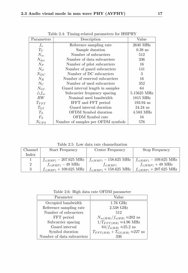
2.3.2 Forward error correctionThis mode of the standard use convolutional encoding. The convolutional encoderdiagram for this standard is depicted in Figure 2.11. The convolutional encoderencode with a code rate of 1/3. The convolutional encoder use 6 delay memory.And generator polynomial g0 = 1338, g1 = 1718andg2 = 1658. The initial value ofthe memories are set to 0.
2.3.3 ModulationThis mode use the same QPSK and 16QAM modulation scheme as shown inFigures 2.8 and 2.9, respectively. This mode also use gray coded input bits.
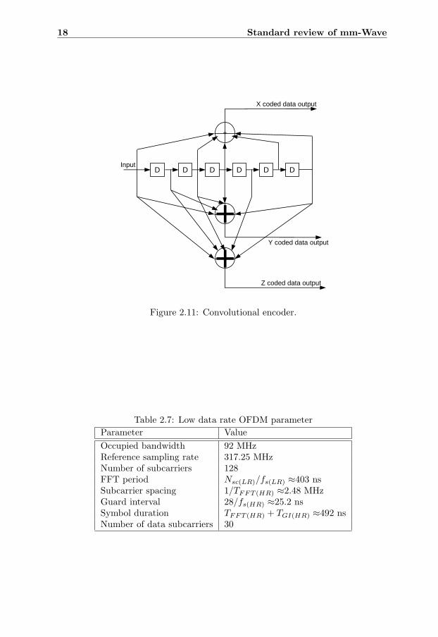
2.3.4 OFDMThis mode use two different OFDM technique for low data rate and high data raterespectively. These are described in Table 2.6 and 2.7 for high data rate and lowdata rate respectively
2.3 Audio visual mode in mm wave PHY (AVPHY) 17
Table 2.4: Timing-related parameters for HSIPHYParameters Description Value
fs Reference sampling rate 2640 MHzTC Sample duration 0.38 nsNsc Number of subcarriers 512Ndsc Number of data subcarriers 336NP Number of pilot subcarriers 16NG Number of guard subcarriers 141
NDC Number of DC subcarriers 3NR Number of reserved subcarriers 16NU Number of used subcarriers 352NGI Guard interval length in samples 644fsc Subcarrier frequency spacing 5.15625 MHzBW Nominal used bandwidth 1815 MHzTFFT IFFT and FFT period 193.94 nsTGI Guard interval duration 24.24 nsTS OFDM Symbol duration 4.583 MHzFS OFDM Symbol rate 16
NCPS Number of samples per OFDM symbols 576
Table 2.5: Low data rate channelizationChannel Start Frequency Center Frequency Stop Frequency
Index1 fc(HRP ) − 207.625 MHz fc(HRP ) − 158.625 MHz fc(HRP ) − 109.625 MHz2 fc(HRP ) − 49 MHz fc(HRP ) fc(HRP ) + 49 MHz3 fc(HRP ) + 109.625 MHz fc(HRP ) + 158.625 MHz fc(HRP ) + 207.625 MHz
Table 2.6: High data rate OFDM parameterParameter Value
Occupied bandwidth 1.76 GHzReference sampling rate 2.538 GHzNumber of subcarriers 512
FFT period Nsc(HR)/fs(HR) ≈202 nsSubcarrier spacing 1/TFFT (HR) ≈4.96 MHz
Guard interval 64/fs(HR) ≈25.2 nsSymbol duration TFFT (HR) + TGI(HR) ≈227 ns
Number of data subcarriers 336
18 Standard review of mm-Wave
DDD DD D
+
++
Input
X coded data output
Y coded data output
Z coded data output
Figure 2.11: Convolutional encoder.
Table 2.7: Low data rate OFDM parameterParameter ValueOccupied bandwidth 92 MHzReference sampling rate 317.25 MHzNumber of subcarriers 128FFT period Nsc(LR)/fs(LR) ≈403 nsSubcarrier spacing 1/TFFT (HR) ≈2.48 MHzGuard interval 28/fs(HR) ≈25.2 nsSymbol duration TFFT (HR) + TGI(HR) ≈492 nsNumber of data subcarriers 30
Chapter 3
High Level Model of IEEE802.15.3c (HSIPHY)
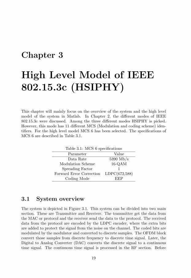
This chapter will mainly focus on the overview of the system and the high levelmodel of the system in Matlab. In Chapter 2, the different modes of IEEE802.15.3c were discussed. Among the three different modes HSIPHY is picked.However, this mode has 11 different MCS (Modulation and coding scheme) iden-tifiers. For the high level model MCS 6 has been selected. The specifications ofMCS 6 are described in Table 3.1.
Table 3.1: MCS 6 specificationsParameter ValueData Rate 5390 Mb/s
Modulation Scheme 16-QAMSpreading Factor 1
Forward Error Correction LDPC(672,588)Coding Mode EEP
3.1 System overview
The system is depicted in Figure 3.1. This system can be divided into two mainsection. These are Transmitter and Receiver. The transmitter get the data fromthe MAC or protocol and the receiver send the data to the protocol. The receiveddata from the protocol are encoded by the LDPC encoder, where the extra bitsare added to protect the signal from the noise on the channel. The coded bits aremodulated by the modulator and converted to discrete samples. The OFDM blockconvert those samples from discrete frequency to discrete time signal. Later, theDigital to Analog Converter (DAC) converts the discrete signal to a continuoustime signal. The continuous time signal is processed in the RF section. Before
19
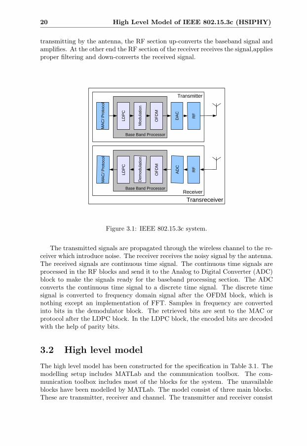
20 High Level Model of IEEE 802.15.3c (HSIPHY)
transmitting by the antenna, the RF section up-converts the baseband signal andamplifies. At the other end the RF section of the receiver receives the signal,appliesproper filtering and down-converts the received signal.
LDP
C
OF
DM
Transmitter
Receiver
Transreceiver
LDP
C
OF
DM
Base Band Processor
MA
C/
Pro
toc o
lM
AC
/ Pro
toc o
l
Base Band Processor
Figure 3.1: IEEE 802.15.3c system.
The transmitted signals are propagated through the wireless channel to the re-ceiver which introduce noise. The receiver receives the noisy signal by the antenna.The received signals are continuous time signal. The continuous time signals areprocessed in the RF blocks and send it to the Analog to Digital Converter (ADC)block to make the signals ready for the baseband processing section. The ADCconverts the continuous time signal to a discrete time signal. The discrete timesignal is converted to frequency domain signal after the OFDM block, which isnothing except an implementation of FFT. Samples in frequency are convertedinto bits in the demodulator block. The retrieved bits are sent to the MAC orprotocol after the LDPC block. In the LDPC block, the encoded bits are decodedwith the help of parity bits.
3.2 High level model
The high level model has been constructed for the specification in Table 3.1. Themodelling setup includes MATLab and the communication toolbox. The com-munication toolbox includes most of the blocks for the system. The unavailableblocks have been modelled by MATLab. The model consist of three main blocks.These are transmitter, receiver and channel. The transmitter and receiver consist
3.2 High level model 21
of forward error correction (FEC) as LDPC(672,588), modulator as 16-QAM andOFDM as a subcomponents.
3.2.1 Transmitter and receiverForward error correction (FEC)
Forward error correction has been used on both transmitter and receiver. TheLDPC object of communication toolbox has been used for this case. LDPC(672,588) follows the standard [1]. The table and the permuted identity matri-ces have been generated in Matlab. The table consist of the zero matrices andpermuted identity matrices.
Modulation and demodulation
Modulation and demodulation convert the bits into samples as well as samples intobits respectively. Modulation has been done on the transmitter and demodulationon the receiver. 16-QAM modulation and demodulation have been performedfor this model. There are modem.qammod, modem.qamdemod, modulate anddemodulate function in the communication toolbox to perform the modulation anddemodulation. The arguments for modem.qammod and modem.qamdemod aredescribed in Table 3.2 and Table 3.3. Later the created objects have been used inmodulate and demodulate function to perform the modulation and demodulation.
Table 3.2: Argument for modem.qammodArgument Description Value
M Modulation index 16PhaseOffset Offset phase of the mapping π/2
SymbolOrder Symbol order of the input grayInputType Type of input bit
Table 3.3: Argument for modem.qamdemodArgument Description Value
M Modulation index 16PhaseOffset Offset phase of the mapping π/2
SymbolOrder Symbol order of the input grayInputType Type of input bit
DecisionType Type of decision LLRNoiseVariance Noise Variance of system 1.2
Orthogonal frequency division multiplexing (OFDM)
The OFDM block has been modelled using IFFT and FFT on transmitter andreceiver, respectively. 141 null subcarriers, 3 DC subcarriers, 16 pilot sub-carriers
22 High Level Model of IEEE 802.15.3c (HSIPHY)
and 16 guard subcarriers have been added with the 336 data subcarriers before theIFFT on the transmitter. In the receiver, the data subcarriers have been extractedfrom the 512 sub-carriers.
3.2.2 ChannelThe processed signal is transmitted through the channel. The channel is wirelessand it has multipath fading effect. The channel can be characterized in two ways.One is large scale characterization and the other is small scale characterization [2].Large scale characterization has been applied here, as in Equation 3.1. The pathloss PL(d) can be defined by the average path loss PL(d) and shadowing fadingXσ.
PL(d)[dB] = PL(d)[dB] + Xσ[dB] (3.1)
However, the average pathloss PL(d) can be expressed as in Equation 3.2. Whered0 and n denote the reference distance and PL exponent. The pathloss exponentn varies for different enviroment. This model has been modeled for the roomenviroment. Xq is for the additional attenuation due to specific obstruction byobjects.
PL(d)[dB] = PL(d0)[dB] + 10n log10
(d
d0
)+
Q∑q=1
Xq, . . . for d ≥ d0 (3.2)
3.3 Performance evaluationTwo different performance measures have been observed in this model. One isBER as a function of SNR and the second one is BER as a function of wordlengthin the FFT. These are described in the following subsections.
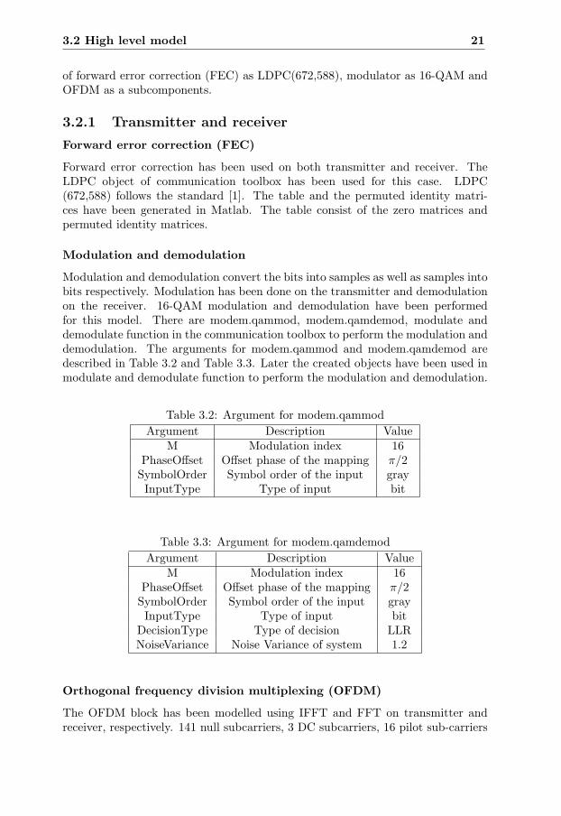
3.3.1 SNR vs BERThe BER has improved with the SNR of the system. The graph in Figure 3.2shows the results for different wordlength. BER of the model reduced with inincrement of the SNR. Figure 3.2 shows the blue line for wordlength 8, the redline for wordlength 12 and the black line for wordlength 16. So, to achieve somenumber of BER the SNR can be selected for a specific wordlength.
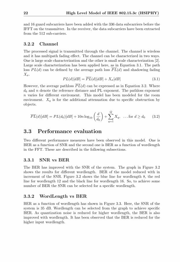
3.3.2 WordLength vs BERBER as a function of wordlength has shown in Figure 3.3. Here, the SNR of thesystem is 35 dB. Wordlength can be selected from the graph to achieve specificBER. As quantization noise is reduced for higher wordlength, the BER is alsoimproved with wordlength. It has been observed that the BER is reduced for thehigher input wordlength.
3.3 Performance evaluation 23
0 5 10 15 20 25 30 35 4010
−6
10−5
10−4
10−3
10−2
10−1
100
Signal to NoiseRatio(dB)
Bit
Err
or R
ate
(BE
R)
8 bit12 bit16 bit
Figure 3.2: BER as a function of SNR.
2 4 6 8 10 12 14 16 1810
−5
10−4
10−3
10−2
10−1
100
Wordlength
Bit
Err
or R
ate
(BE
R)
Figure 3.3: BER as a Function of Wordlength at SNR 35 dB.

Chapter 4
Background of FFT
A short description of the FFT algorithm, different architectures and the basicbuilding blocks for the architectures are discussed in this chapter. Further infor-mation about the algorithm and architectures are discussed in [3–7].
4.1 Theoretical backgroundSome claim that 1965 is the start of the modern world, when J. Cooley and J.Tukey published their efficient method for numerical computation of the Fouriertransform. Some others claim, the method was introduced by Gauss in the mid1800s, the idea that lies at the heart of the algorithm is clearly present in anunpublished paper that appeared posthumously in 1866. However, the presentand future demands are that now a days people process continuous signals bydiscrete methods. Computers and digital processing systems can not work withcontinuous sums. The FFT represent a general function in terms of summation oftrigonometric functions. This mathematical operation transforms the time domainsignal into frequency domain signal according to the DFT:
X[k] =N∑
n=0
x[n]W knN , k = 0...N − 1 (4.1)
In Equation 4.1 X[k] and x[n] are the complex output and the input of N pointFFT respectively, where n is the time index and k is the frequency index. W kn
N isthe twiddle factor. W kn
N can be defined as in Equation 4.2.
W knN = e−j(2πkn/N) = cos(
2πkn
N)− j · sin(
2πkn
N) (4.2)
For a better understanding of the operations performed by the FFT, the FFTis represented by its signal flow graph (SFG). Examples of signal flow graphsare shown in Figures 4.1, 4.2, 4.3 and 4.4. The SFGs in the Figures consist ofbutterflies and complex rotations. For examples Figure 4.1 represents a radix-2butterfly, which computes:
25
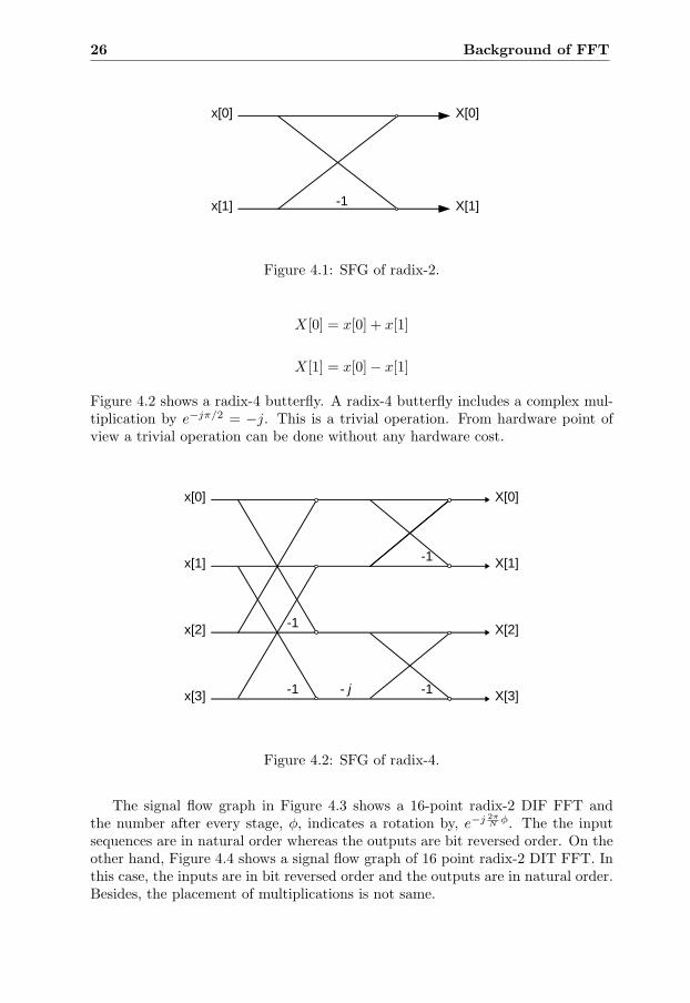
26 Background of FFT
Figure 4.1: SFG of radix-2.
X[0] = x[0] + x[1]
X[1] = x[0]− x[1]
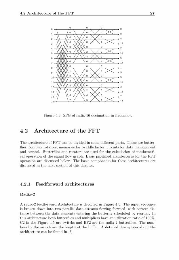
Figure 4.2 shows a radix-4 butterfly. A radix-4 butterfly includes a complex mul-tiplication by e−jπ/2 = −j. This is a trivial operation. From hardware point ofview a trivial operation can be done without any hardware cost.
Figure 4.2: SFG of radix-4.
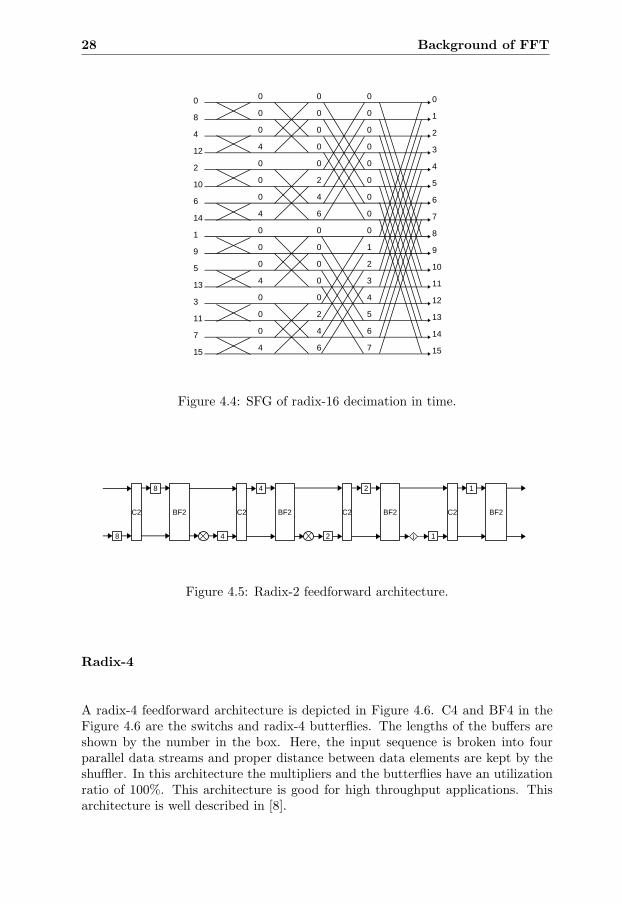
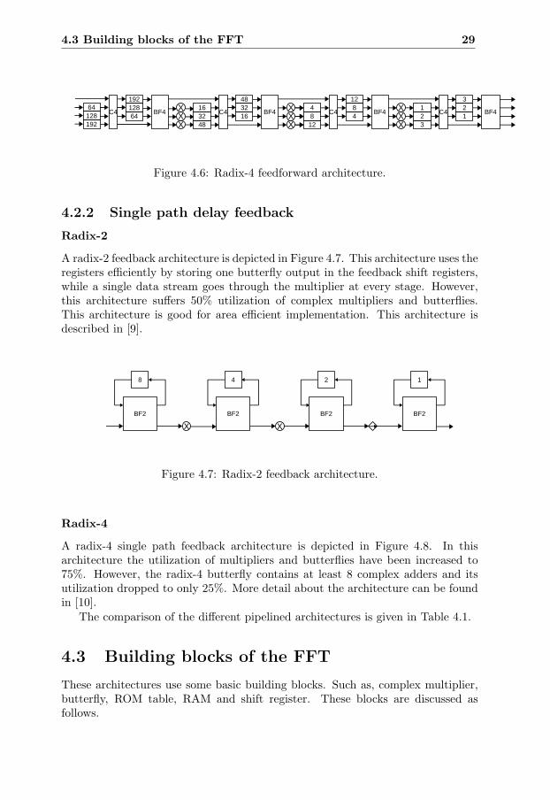
The signal flow graph in Figure 4.3 shows a 16-point radix-2 DIF FFT andthe number after every stage, φ, indicates a rotation by, e−j 2π
N φ. The the inputsequences are in natural order whereas the outputs are bit reversed order. On theother hand, Figure 4.4 shows a signal flow graph of 16 point radix-2 DIT FFT. Inthis case, the inputs are in bit reversed order and the outputs are in natural order.Besides, the placement of multiplications is not same.
4.2 Architecture of the FFT 27
00
0
0
0
0
0
0
0
0
0
0
0
0
0
0
0
0
0
0
0
0
0
0
0
0
0
0
0
0
0
1
2
3
4
5
6
7
2
4
6
2
4
6
4
4
4
4
0
1
2
3
4
5
6
7
8
9
10
11
12
13
14
15
0
8
4
12
2
10
6
14
1
9
5
13
3
11
7
15
Figure 4.3: SFG of radix-16 decimation in frequency.
4.2 Architecture of the FFT
The architecture of FFT can be divided in some different parts. Those are butter-flies, complex rotators, memories for twiddle factor, circuits for data managementand control. Butterflies and rotators are used for the calculation of mathemati-cal operation of the signal flow graph. Basic pipelined architectures for the FFToperation are discussed below. The basic components for these architectures arediscussed in the next section of this chapter.
4.2.1 Feedforward architectures
Radix-2
A radix-2 feedforward Architecture is depicted in Figure 4.5. The input sequenceis broken down into two parallel data streams flowing forward, with correct dis-tance between the data elements entering the butterfly scheduled by reorder. Inthis architecture both butterflies and multipliers have an utilization ratio of 100%.C2 in the Figure 4.5 are switchs and BF2 are the radix-2 butterflies. The num-bers by the switch are the length of the buffer. A detailed description about thearchitecture can be found in [3].
28 Background of FFT
00
0
0
4
0
0
0
4
0
0
0
0
0
0
0
0
0
0
0
0
0
0
0
0
0
1
2
4
5
6
0
2
4
6
0
0
3
7
0
1
2
3
4
5
6
7
8
9
10
11
12
13
14
15
0
8
4
12
2
10
6
14
1
9
5
13
3
11
7
15
0
0
4
0
0
4
2
4
6
Figure 4.4: SFG of radix-16 decimation in time.
j
Figure 4.5: Radix-2 feedforward architecture.
Radix-4
A radix-4 feedforward architecture is depicted in Figure 4.6. C4 and BF4 in theFigure 4.6 are the switchs and radix-4 butterflies. The lengths of the buffers areshown by the number in the box. Here, the input sequence is broken into fourparallel data streams and proper distance between data elements are kept by theshuffler. In this architecture the multipliers and the butterflies have an utilizationratio of 100%. This architecture is good for high throughput applications. Thisarchitecture is well described in [8].
4.3 Building blocks of the FFT 29
C4 C4 C4 C4BF4 BF4 BF4 BF4
19212864
163248
483216
123
4812
123
XXX
XXX
XXX
4812192
12864
Figure 4.6: Radix-4 feedforward architecture.
4.2.2 Single path delay feedback
Radix-2
A radix-2 feedback architecture is depicted in Figure 4.7. This architecture uses theregisters efficiently by storing one butterfly output in the feedback shift registers,while a single data stream goes through the multiplier at every stage. However,this architecture suffers 50% utilization of complex multipliers and butterflies.This architecture is good for area efficient implementation. This architecture isdescribed in [9].
Figure 4.7: Radix-2 feedback architecture.
Radix-4
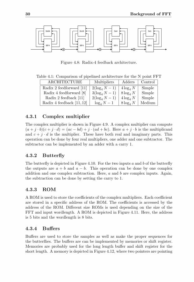
A radix-4 single path feedback architecture is depicted in Figure 4.8. In thisarchitecture the utilization of multipliers and butterflies have been increased to75%. However, the radix-4 butterfly contains at least 8 complex adders and itsutilization dropped to only 25%. More detail about the architecture can be foundin [10].
The comparison of the different pipelined architectures is given in Table 4.1.
4.3 Building blocks of the FFT
These architectures use some basic building blocks. Such as, complex multiplier,butterfly, ROM table, RAM and shift register. These blocks are discussed asfollows.
30 Background of FFT
Figure 4.8: Radix-4 feedback architecture.
Table 4.1: Comparison of pipelined architecture for the N point FFTARCHITECTURE Multipliers Adders Control
Radix 2 feedforward [11] 2(log4 N − 1) 4 log4 N SimpleRadix 4 feedforward [8] 3(log4 N − 1) 8 log4 N SimpleRadix 2 feedback [11] 2(log4 N − 1) 4 log4 N Simple
Radix 4 feedback [11,12] log4 N − 1 8 log4 N Medium
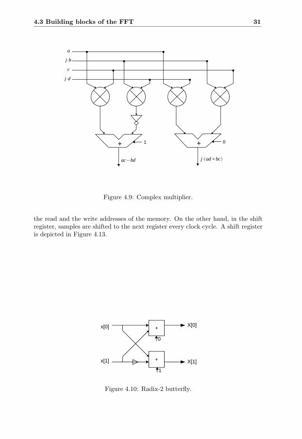
4.3.1 Complex multiplierThe complex multiplier is shown in Figure 4.9. A complex multiplier can compute(a + j · b)(c + j · d) = (ac − bd) + j · (ad + bc). Here a + j · b is the multiplicandand c + j · d is the multiplier. These have both real and imaginary parts. Thisoperation can be done by four real multipliers, one adder and one subtractor. Thesubtractor can be implemented by an adder with a carry 1.
4.3.2 ButterflyThe butterfly is depicted in Figure 4.10. For the two inputs a and b of the butterflythe outputs are a + b and a − b. This operation can be done by one complexaddition and one complex subtraction. Here, a and b are complex inputs. Again,the subtraction can be done by setting the carry to 1.
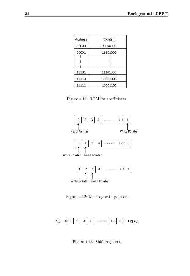
4.3.3 ROMA ROM is used to store the coefficients of the complex multipliers. Each coefficientare stored in a specific address of the ROM. The coefficients is accessed by theaddress of the ROM. Different size ROMs is used depending on the size of theFFT and input wordlength. A ROM is depicted in Figure 4.11. Here, the addressis 5 bits and the wordlength is 8 bits.
4.3.4 BuffersBuffers are used to store the samples as well as make the proper sequences forthe butterflies. The buffers are can be implemented by memories or shift register.Memories are probably used for the long length buffer and shift register for theshort length. A memory is depicted in Figure 4.12, where two pointers are pointing
4.3 Building blocks of the FFT 31
Figure 4.9: Complex multiplier.
the read and the write addresses of the memory. On the other hand, in the shiftregister, samples are shifted to the next register every clock cycle. A shift registeris depicted in Figure 4.13.
+
+
0
1
x[0]
x[1]
X[0]
X[1]
Figure 4.10: Radix-2 butterfly.
32 Background of FFT
Address Content
00000
00001
11101
11110
11111
00000000
11101000
11101000
10001000
10001100
Figure 4.11: ROM for coefficients.
Read Pointer
Read Pointer
Read Pointer
Write Pointer
Write Pointer
Write Pointer
Figure 4.12: Memory with pointer.
2 3 4 L-1 L1X[i] X[i+L]
Figure 4.13: Shift registers.
Chapter 5
Implementation of FFT onASIC
This chapter focuses on the implementation of an FFT for the IEEE 802.15.3c(HSIPHY mode) standard. CORE65LPSVT technology library has been used forthis implementation. This library is mainly used for ultra low power applications.For this implementation, 0.8 V supply voltage and a 330 MHZ clock have beenused. Table 5.1 shows the specification of the ASIC. The specifications for theFFT are noted in [1]. The FFT shall be 512 point and the sample rate 2.64 GS/s.In order to meet the requirement of the throughput, 8 parallel samples have beenused as input of the FFT. Table 5.2 shows the requirements of the FFT. Among512 sub-carriers, 336 are data sub-carriers, 16 are pilot sub-carriers, 16 are guardsub-carriers, 3 are DC sub-carriers and 141 are Null sub-carriers.
Table 5.1: Constraint of the ASICASIC Constraint Value
Library CORE65LPSVTProcess 65 nm
Global Power Supply 0.8 VGlobal Clock Frequency 330 MHz
Table 5.2: Design constraint of the FFTDesign Parameter ValueLength of the FFT 512
sample rate 2.64 GS/sSamples in parallel 8
33
34 Implementation of FFT on ASIC
5.1 Design issue related to the FFT processorFFT architectures can be divided into two different categories: pipelined ar-chitectures (such that feedforward and feedback) and memory-based architec-tures. These architectures are described in [7, 13–15] and [16–18] respectively.On one hand, pipelined architectures have the advantage of high throughput.However, these architectures have high area cost for large point FFTs. On theother hand, memory-based architectures have advantage of low area cost, butoften the throughput is limited due to the memory access bandwidth and theavailable number of processing elements. In order to meet the requirements ofIEEE 802.15.3c standard, a high throughput FFT processor needs to be designed.For high throughput applications, a pipelined FFT architecture has been adoptedmost times.
Among different pipelined architectures, single path delay feedback architec-tures have the advantages of less number of memories and hardware comparedto multipath feedforward architectures. However, single path delay feedback ar-chitectures use the processing unit for 50% compared to multipath feedforwardarchitectures. On the other hand, multipath feedforward architectures can processtwo or more samples in parallel, whereas single path feedback ones only processone sample per clock cycle. Therefore, feedforward architectures can operate atslower clock than feedback architectures. For a slower clock, low power can beacheived for feedforward architectures. However, these architectures increase thehardware cost significantly, as more complex rotators, butterflies and memoriesare needed. The above listed architectures have some advantage and some com-mon requirement, as has been well described in [19–21]. A radix-8 and 8 paralleldata architecture has been proposed for this application. As the throughput of theFFT is quite high, 8 parallel data can reduce the clock frequency and the directimplementation of radix-8 butterfly need 8 parallel data. Besides, the proposedarchitecture reduces the number of multipliers and complex adders.
Finally, the processing elements of the data path can operate at maximum 500MHz (2 ns delay) clock frequency. Therefore, a 330 MHz clock has been used forthe pipeline architecture, and 8 parallel samples are the good choice to reduce theinput clock frequency.
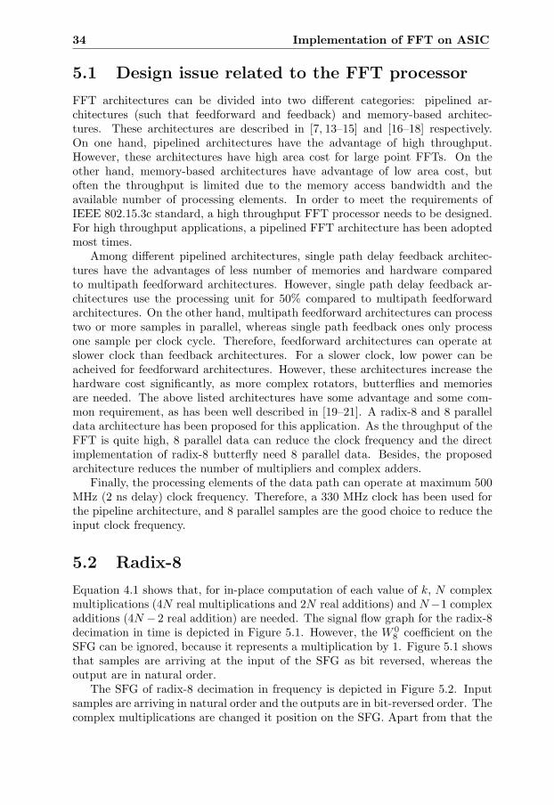
5.2 Radix-8Equation 4.1 shows that, for in-place computation of each value of k, N complexmultiplications (4N real multiplications and 2N real additions) and N−1 complexadditions (4N − 2 real addition) are needed. The signal flow graph for the radix-8decimation in time is depicted in Figure 5.1. However, the W 0
8 coefficient on theSFG can be ignored, because it represents a multiplication by 1. Figure 5.1 showsthat samples are arriving at the input of the SFG as bit reversed, whereas theoutput are in natural order.
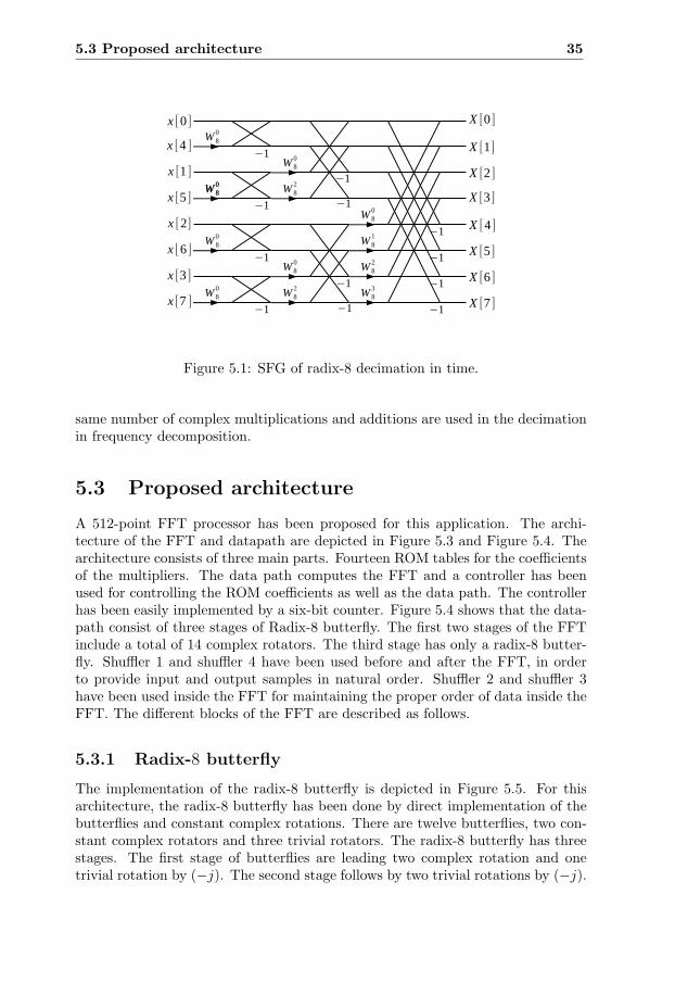
The SFG of radix-8 decimation in frequency is depicted in Figure 5.2. Inputsamples are arriving in natural order and the outputs are in bit-reversed order. Thecomplex multiplications are changed it position on the SFG. Apart from that the
5.3 Proposed architecture 35
W 80
W 80
W 80
W 80
W 80
W 80
W 80
W 82
W 82
W 80
W 81
W 82
W 83
X [0 ]
x [1 ]
x [2]
x [3 ]
x [4 ]
x [5 ]
x [7 ]
x [6 ]
X [1]
x [0 ]
X [2 ]
X [3 ]
X [4 ]
X [5 ]
X [6 ]
X [7 ]
−1
−1
−1
−1
−1
−1
−1
−1
−1
−1
−1
−1
Figure 5.1: SFG of radix-8 decimation in time.
same number of complex multiplications and additions are used in the decimationin frequency decomposition.
5.3 Proposed architecture
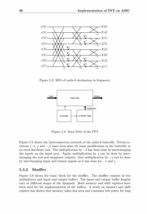
A 512-point FFT processor has been proposed for this application. The archi-tecture of the FFT and datapath are depicted in Figure 5.3 and Figure 5.4. Thearchitecture consists of three main parts. Fourteen ROM tables for the coefficientsof the multipliers. The data path computes the FFT and a controller has beenused for controlling the ROM coefficients as well as the data path. The controllerhas been easily implemented by a six-bit counter. Figure 5.4 shows that the data-path consist of three stages of Radix-8 butterfly. The first two stages of the FFTinclude a total of 14 complex rotators. The third stage has only a radix-8 butter-fly. Shuffler 1 and shuffler 4 have been used before and after the FFT, in orderto provide input and output samples in natural order. Shuffler 2 and shuffler 3have been used inside the FFT for maintaining the proper order of data inside theFFT. The different blocks of the FFT are described as follows.
5.3.1 Radix-8 butterfly
The implementation of the radix-8 butterfly is depicted in Figure 5.5. For thisarchitecture, the radix-8 butterfly has been done by direct implementation of thebutterflies and constant complex rotations. There are twelve butterflies, two con-stant complex rotators and three trivial rotators. The radix-8 butterfly has threestages. The first stage of butterflies are leading two complex rotation and onetrivial rotation by (−j). The second stage follows by two trivial rotations by (−j).
36 Implementation of FFT on ASIC
W 80
W 80
W 80
W 81
W 82
W 83
W 82
W 82
x [1 ]
x [2]
x [3 ]
x [4 ]
x [5 ]
x [7 ]
x [6 ]
x [0 ] X [0 ]
X [1]
X [2 ]
X [3 ]
X [4 ]
X [5 ]
X [6 ]
X [7 ]
−1
−1
−1
−1
−1
−1
−1
−1
−1
−1
−1
−1
Figure 5.2: SFG of radix-8 decimation in frequency.
Data Path
14 ROM TableController
Input Output
Coefficient
Figure 5.3: Data Path of the FFT
Figure 5.5 shows the interconnection network of the radix-8 butterfly. Trivial ro-tations (−1, j and −j) have been done by some modification in the butterfly atno extra hardware cost. The multiplication by −1 has been done by interchangingthe inputs on the input port. Again, multiplication by j can be done by inter-changing the real and imaginary outputs. And multiplication by −j can be doneby interchanging input and output signals as it has done for −1 and j.
5.3.2 ShufflerFigure 5.6 shows the basic block for the shuffler. The shuffler consists of twomultiplexers and input and output buffers. The input and output buffer lengthsvary at different stages of the datapath. Both memory and shift registers havebeen used for the implementation of the buffers. A study on memory and shiftregister has shown that memory takes less area and consumes less power for long
5.3 Proposed architecture 37
X
X
X
X
X
X
X
X
X
X
X
X
X
X
x[0]
x[1]
x[2]
x[3]
x[4]
x[5]
x[6]
x[7]
X[0]
X[1]
X[2]
X[3]
X[4]
X[5]
X[6]
X[7]
Figure 5.4: Data path of the FFT.
Butterfly
Butterfly
Butterfly
Butterfly
Butterfly
Butterfly
Butterfly
Butterfly
Butterfly
Butterfly
Butterfly
Butterfly
x
X
X
x
x
x[0]
x[1]
x[2]
x[3]
x[4]
x[5]
x[6]
x[7]
x[0]
x[4]
x[1]
x[5]
x[2]
x[6]
x[3]
x[7]
Figure 5.5: Implementation of radix-8 butterfly.
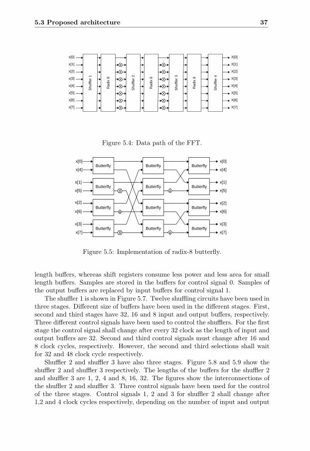
length buffers, whereas shift registers consume less power and less area for smalllength buffers. Samples are stored in the buffers for control signal 0. Samples ofthe output buffers are replaced by input buffers for control signal 1.
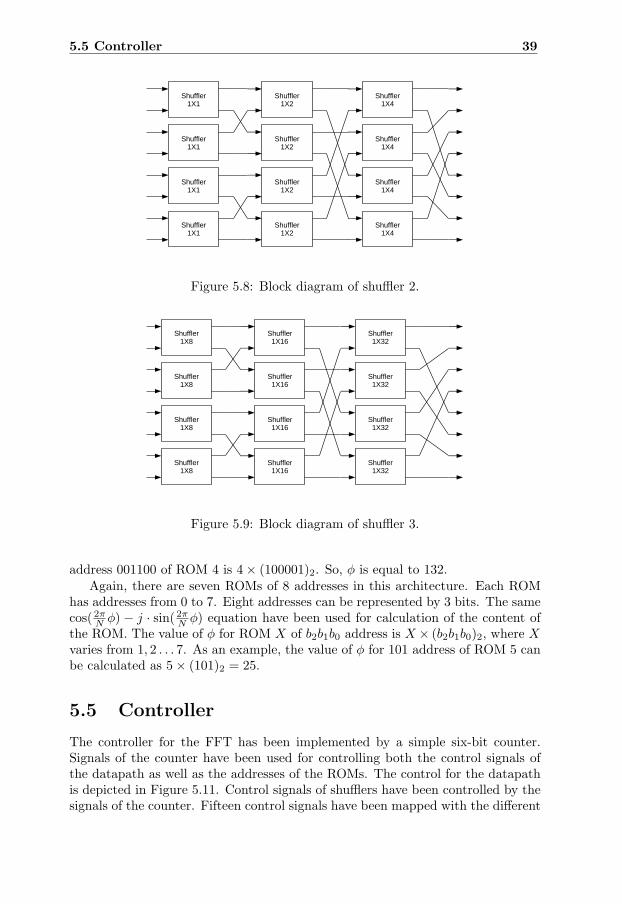
The shuffler 1 is shown in Figure 5.7. Twelve shuffling circuits have been used inthree stages. Different size of buffers have been used in the different stages. First,second and third stages have 32, 16 and 8 input and output buffers, respectively.Three different control signals have been used to control the shufflers. For the firststage the control signal shall change after every 32 clock as the length of input andoutput buffers are 32. Second and third control signals must change after 16 and8 clock cycles, respectively. However, the second and third selections shall waitfor 32 and 48 clock cycle respectively.
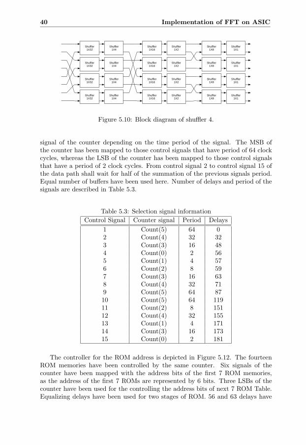
Shuffler 2 and shuffler 3 have also three stages. Figure 5.8 and 5.9 show theshuffler 2 and shuffler 3 respectively. The lengths of the buffers for the shuffler 2and shuffler 3 are 1, 2, 4 and 8, 16, 32. The figures show the interconnections ofthe shuffler 2 and shuffler 3. Three control signals have been used for the controlof the three stages. Control signals 1, 2 and 3 for shuffler 2 shall change after1,2 and 4 clock cycles respectively, depending on the number of input and output
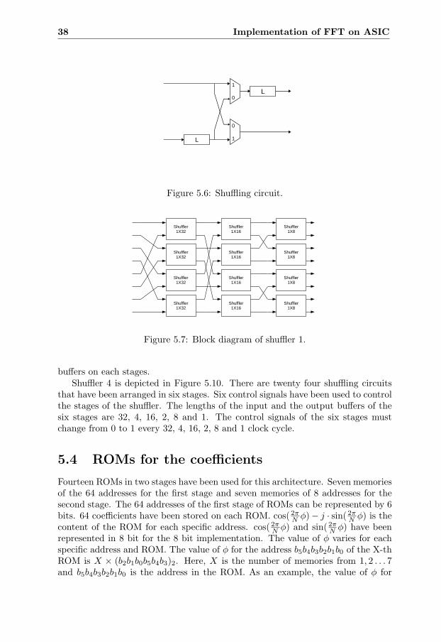
38 Implementation of FFT on ASIC
L
L
1
0
1
0
Figure 5.6: Shuffling circuit.
Shuffler1X32
Shuffler1X32
Shuffler1X32
Shuffler1X32
Shuffler1X16
Shuffler1X16
Shuffler1X16
Shuffler1X16
Shuffler1X8
Shuffler1X8
Shuffler1X8
Shuffler1X8
Figure 5.7: Block diagram of shuffler 1.
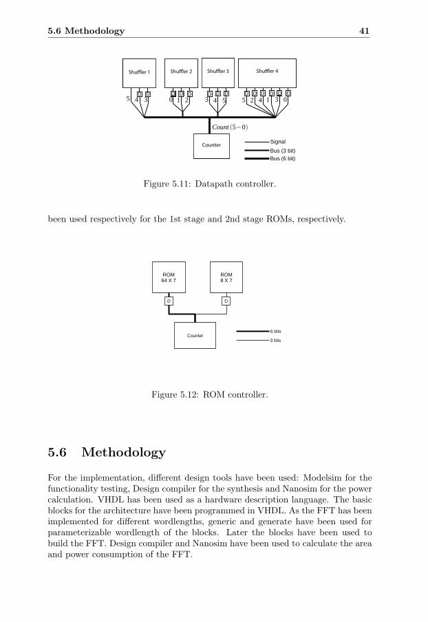
buffers on each stages.Shuffler 4 is depicted in Figure 5.10. There are twenty four shuffling circuits
that have been arranged in six stages. Six control signals have been used to controlthe stages of the shuffler. The lengths of the input and the output buffers of thesix stages are 32, 4, 16, 2, 8 and 1. The control signals of the six stages mustchange from 0 to 1 every 32, 4, 16, 2, 8 and 1 clock cycle.
5.4 ROMs for the coefficients
Fourteen ROMs in two stages have been used for this architecture. Seven memoriesof the 64 addresses for the first stage and seven memories of 8 addresses for thesecond stage. The 64 addresses of the first stage of ROMs can be represented by 6bits. 64 coefficients have been stored on each ROM. cos( 2π
N φ)− j · sin( 2πN φ) is the
content of the ROM for each specific address. cos( 2πN φ) and sin( 2π
N φ) have beenrepresented in 8 bit for the 8 bit implementation. The value of φ varies for eachspecific address and ROM. The value of φ for the address b5b4b3b2b1b0 of the X-thROM is X × (b2b1b0b5b4b3)2. Here, X is the number of memories from 1, 2 . . . 7and b5b4b3b2b1b0 is the address in the ROM. As an example, the value of φ for
5.5 Controller 39
Shuffler1X1
Shuffler1X1
Shuffler1X1
Shuffler1X1
Shuffler1X2
Shuffler1X2
Shuffler1X2
Shuffler1X2
Shuffler1X4
Shuffler1X4
Shuffler1X4
Shuffler1X4
Figure 5.8: Block diagram of shuffler 2.
Shuffler1X8
Shuffler1X8
Shuffler1X8
Shuffler1X8
Shuffler1X16
Shuffler1X16
Shuffler1X16
Shuffler1X16
Shuffler1X32
Shuffler1X32
Shuffler1X32
Shuffler1X32
Figure 5.9: Block diagram of shuffler 3.
address 001100 of ROM 4 is 4× (100001)2. So, φ is equal to 132.Again, there are seven ROMs of 8 addresses in this architecture. Each ROM
has addresses from 0 to 7. Eight addresses can be represented by 3 bits. The samecos( 2π
N φ) − j · sin( 2πN φ) equation have been used for calculation of the content of
the ROM. The value of φ for ROM X of b2b1b0 address is X × (b2b1b0)2, where Xvaries from 1, 2 . . . 7. As an example, the value of φ for 101 address of ROM 5 canbe calculated as 5× (101)2 = 25.
5.5 Controller
The controller for the FFT has been implemented by a simple six-bit counter.Signals of the counter have been used for controlling both the control signals ofthe datapath as well as the addresses of the ROMs. The control for the datapathis depicted in Figure 5.11. Control signals of shufflers have been controlled by thesignals of the counter. Fifteen control signals have been mapped with the different
40 Implementation of FFT on ASIC
Shuffler1X32
Shuffler1X32
Shuffler1X32
Shuffler1X32
Shuffler1X4
Shuffler1X4
Shuffler1X4
Shuffler1X4
Shuffler1X16
Shuffler1X16
Shuffler1X16
Shuffler1X16
Shuffler1X2
Shuffler1X2
Shuffler1X2
Shuffler1X2
Shuffler1X1
Shuffler1X1
Shuffler1X1
Shuffler1X1
Shuffler1X8
Shuffler1X8
Shuffler1X8
Shuffler1X8
Figure 5.10: Block diagram of shuffler 4.
signal of the counter depending on the time period of the signal. The MSB ofthe counter has been mapped to those control signals that have period of 64 clockcycles, whereas the LSB of the counter has been mapped to those control signalsthat have a period of 2 clock cycles. From control signal 2 to control signal 15 ofthe data path shall wait for half of the summation of the previous signals period.Equal number of buffers have been used here. Number of delays and period of thesignals are described in Table 5.3.
Table 5.3: Selection signal informationControl Signal Counter signal Period Delays
1 Count(5) 64 02 Count(4) 32 323 Count(3) 16 484 Count(0) 2 565 Count(1) 4 576 Count(2) 8 597 Count(3) 16 638 Count(4) 32 719 Count(5) 64 8710 Count(5) 64 11911 Count(2) 8 15112 Count(4) 32 15513 Count(1) 4 17114 Count(3) 16 17315 Count(0) 2 181
The controller for the ROM address is depicted in Figure 5.12. The fourteenROM memories have been controlled by the same counter. Six signals of thecounter have been mapped with the address bits of the first 7 ROM memories,as the address of the first 7 ROMs are represented by 6 bits. Three LSBs of thecounter have been used for the controlling the address bits of next 7 ROM Table.Equalizing delays have been used for two stages of ROM. 56 and 63 delays have
5.6 Methodology 41
Shu�er 1 Shu�er 2 Shu�er 3 Shu�er 4
Counter
D D D D D D D D D D D D D D
Figure 5.11: Datapath controller.
been used respectively for the 1st stage and 2nd stage ROMs, respectively.
Counter
D
ROM64 X 7
D
ROM8 X 7
6 bits
3 bits
Figure 5.12: ROM controller.
5.6 Methodology
For the implementation, different design tools have been used: Modelsim for thefunctionality testing, Design compiler for the synthesis and Nanosim for the powercalculation. VHDL has been used as a hardware description language. The basicblocks for the architecture have been programmed in VHDL. As the FFT has beenimplemented for different wordlengths, generic and generate have been used forparameterizable wordlength of the blocks. Later the blocks have been used tobuild the FFT. Design compiler and Nanosim have been used to calculate the areaand power consumption of the FFT.
42 Implementation of FFT on ASIC
5.6.1 Hardware implementation in VHDL
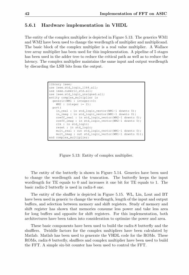
The entity of the complex multiplier is depicted in Figure 5.13. The generics WM1and WM2 have been used to change the wordlength of multiplier and multiplicand.The basic block of the complex multiplier is a real value multiplier. A Wallacetree array multiplier has been used for this implementation. A pipeline of 5 stageshas been used in the adder tree to reduce the critical path as well as to reduce thelatency. The complex multiplier maintains the same input and output wordlengthby discarding the LSB bits from the output.
library ieee;use ieee.std_logic_1164.all;use ieee.numeric_std.all;use ieee.std_logic_unsigned.all;entity complex_multiplier is generic(WM1 : integer:=3; WM2 : integer := 2); port( in_real : in std_logic_vector(WM1-1 downto 0); in_imag : in std_logic_vector(WM1-1 downto 0); coeff_real : in std_logic_vector(WM2-1 downto 0); coeff_imag : in std_logic_vector(WM2-1 downto 0); clk : in std_logic; reset : in std_logic; mult_real : out std_logic_vector(WM1-1 downto 0); mult_imag : out std_logic_vector(WM1-1 downto 0));end complex_multiplier;
Figure 5.13: Entity of complex multiplier.
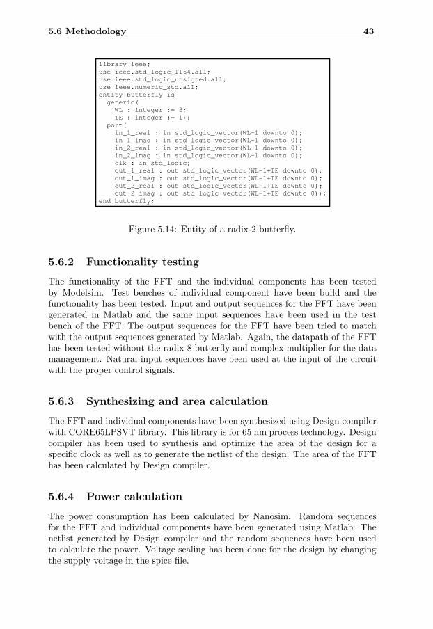
The entity of the butterfly is shown in Figure 5.14. Generics have been usedto change the wordlength and the truncation. The butterfly keeps the inputwordlength for TE equals to 0 and increases it one bit for TE equals to 1. Thebasic radix-2 butterfly is used in radix-8 one.
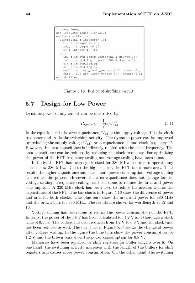
The entity of the shuffler is depicted in Figure 5.15. WL, Lin, Lout and BThave been used in generic to change the wordlength, length of the input and outputbuffers, and selection between memory and shift registers. Study of memory andshift register has shown that memories consume less power and take less areafor long buffers and opposite for shift registers. For this implementation, botharchitectures have been taken into consideration to optimize the power and area.
These basic components have been used to build the radix-8 butterfly and theshufflers. Twiddle factors for the complex multipliers have been calculated byMatlab. Matlab has been used to generate the VHDL code for the ROMs. TheseROMs, radix-8 butterfly, shufflers and complex multiplier have been used to buildthe FFT. A simple six-bit counter has been used to control the FFT.
5.6 Methodology 43
library ieee;use ieee.std_logic_1164.all;use ieee.std_logic_unsigned.all;use ieee.numeric_std.all;entity butterfly is generic( WL : integer := 3; TE : integer := 1); port( in_1_real : in std_logic_vector(WL-1 downto 0); in_1_imag : in std_logic_vector(WL-1 downto 0); in_2_real : in std_logic_vector(WL-1 downto 0); in_2_imag : in std_logic_vector(WL-1 downto 0); clk : in std_logic; out_1_real : out std_logic_vector(WL-1+TE downto 0); out_1_imag : out std_logic_vector(WL-1+TE downto 0); out_2_real : out std_logic_vector(WL-1+TE downto 0); out_2_imag : out std_logic_vector(WL-1+TE downto 0));end butterfly;
Figure 5.14: Entity of a radix-2 butterfly.
5.6.2 Functionality testing
The functionality of the FFT and the individual components has been testedby Modelsim. Test benches of individual component have been build and thefunctionality has been tested. Input and output sequences for the FFT have beengenerated in Matlab and the same input sequences have been used in the testbench of the FFT. The output sequences for the FFT have been tried to matchwith the output sequences generated by Matlab. Again, the datapath of the FFThas been tested without the radix-8 butterfly and complex multiplier for the datamanagement. Natural input sequences have been used at the input of the circuitwith the proper control signals.
5.6.3 Synthesizing and area calculation
The FFT and individual components have been synthesized using Design compilerwith CORE65LPSVT library. This library is for 65 nm process technology. Designcompiler has been used to synthesis and optimize the area of the design for aspecific clock as well as to generate the netlist of the design. The area of the FFThas been calculated by Design compiler.
5.6.4 Power calculation
The power consumption has been calculated by Nanosim. Random sequencesfor the FFT and individual components have been generated using Matlab. Thenetlist generated by Design compiler and the random sequences have been usedto calculate the power. Voltage scaling has been done for the design by changingthe supply voltage in the spice file.
44 Implementation of FFT on ASIC
library ieee;use ieee.std_logic_1164.all;entity shuffler is generic(WL : integer:= 10; Lin : integer := 20; Lout : integer := 10; BT : integer := 1); port( in0 : in std_logic_vector(WL-1 downto 0); in1 : in std_logic_vector(WL-1 downto 0); clk : in std_logic; sel : in std_logic; out0 : out std_logic_vector(WL-1 downto 0); out1 : out std_logic_vector(WL-1 downto 0));end shuffler;
Figure 5.15: Entity of shuffling circuit.
5.7 Design for Low PowerDynamic power of any circuit can be illustrated by:
Pdynamic =12αfcV 2
dd (5.1)
In the equation ‘c’ is the area capacitance, ‘Vdd’ is the supply voltage, ‘f’ is the clockfrequency and ‘α’ is the switching activity. The dynamic power can be improvedby reducing the supply voltage ‘Vdd’, area capacitance ‘c’ and clock frequency ‘f’.However, the area capacitance is indirectly related with the clock frequency. Thearea capacitance can be reduced by reducing the clock frequency. For optimizingthe power of the FFT frequency scaling and voltage scaling have been done.
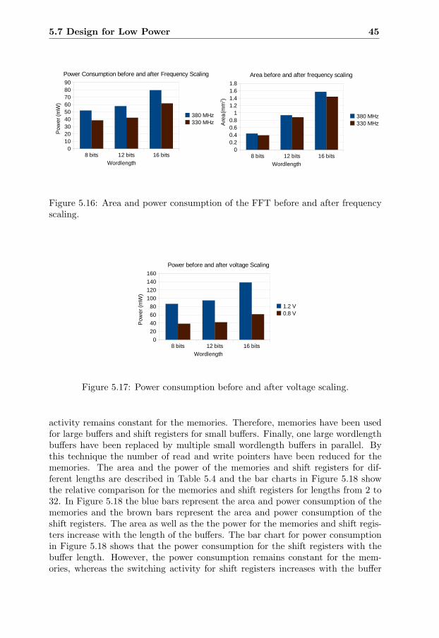
Initially, the FFT has been synthesized for 380 MHz in order to operate anyclock below 380 MHz. Due to the higher clock, the FFT takes more area. Thatresults the higher capacitance and cause more power consumption. Voltage scalingcan reduce the power. However, the area capacitance does not change for thevoltage scaling. Frequency scaling has been done to reduce the area and powerconsumption. A 330 MHz clock has been used to reduce the area as well as thecapacitance of the FFT. The bar charts in Figure 5.16 show the difference of powerand area for both clocks. The blue bars show the area and power for 380 MHzand the brown bars for 330 MHz. The results are shown for wordlength 8, 12 and16.
Voltage scaling has been done to reduce the power consumption of the FFT.Initially, the power of the FFT has been calculated for 1.2 V and there was a slacktime of 0.5 ns. The voltage has been reduced from 1.2 V to 0.8 V and the slack timehas been reduced as well. The bar chart in Figure 5.17 shows the change of powerafter voltage scaling. In the figure the blue bars show the power consumption for1.2 V and the brown bars show the power consumption for 0.8 V.
Memories have been replaced by shift registers for buffer lengths over 8. Onone hand, the switching activity increases with the length of the buffers for shiftregisters and causes more power consumption. On the other hand, the switching
5.7 Design for Low Power 45
8 bits 12 bits 16 bits0
0.20.40.60.8
11.21.41.61.8
Area before and after frequency scaling
380 MHz330 MHz
Wordlength
Are
a
8 bits 12 bits 16 bits0
102030405060708090
Power Consumption before and after Frequency Scaling
380 MHz330 MHz
Wordlength
Po
we
r (m
W)
(mm
2 )
Figure 5.16: Area and power consumption of the FFT before and after frequencyscaling.
8 bits 12 bits 16 bits0
20
40
60
80
100
120
140
160
Power before and after voltage Scaling
1.2 V0.8 V
Wordlength
Po
we
r (m
W)
Figure 5.17: Power consumption before and after voltage scaling.
activity remains constant for the memories. Therefore, memories have been usedfor large buffers and shift registers for small buffers. Finally, one large wordlengthbuffers have been replaced by multiple small wordlength buffers in parallel. Bythis technique the number of read and write pointers have been reduced for thememories. The area and the power of the memories and shift registers for dif-ferent lengths are described in Table 5.4 and the bar charts in Figure 5.18 showthe relative comparison for the memories and shift registers for lengths from 2 to32. In Figure 5.18 the blue bars represent the area and power consumption of thememories and the brown bars represent the area and power consumption of theshift registers. The area as well as the the power for the memories and shift regis-ters increase with the length of the buffers. The bar chart for power consumptionin Figure 5.18 shows that the power consumption for the shift registers with thebuffer length. However, the power consumption remains constant for the mem-ories, whereas the switching activity for shift registers increases with the buffer
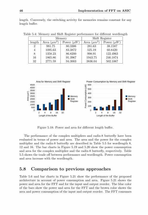
46 Implementation of FFT on ASIC
length. Conversely, the switching activity for memories remains constant for anylength buffer.
Table 5.4: Memory and Shift Register performance for different wordlengthMemory Shift Register
length Area (µm2) Power (µW ) Area (µm2) Power (µW )2 981.75 80.3306 281.63 38.15874 1095.63 83.3872 525.19 60.84208 1358.23 86.8200 998.91 122.496316 1865.86 91.3967 1943.75 246.187432 2771.59 94.3003 3836.04 502.1067
2 4 8 16 320
50010001500200025003000350040004500
Area for Memory and Shift Register
MemoryShift Register
Length of the Buffer
Are
a
2 4 8 16 320
100
200
300
400
500
600
Power Consumption by Memory and Shift Register
MemoryShift Register
Length of the Buffer
Po
we
r C
on
sum
ptio
n
(um
2 )
(uW
)
Figure 5.18: Power and area for different length buffer.
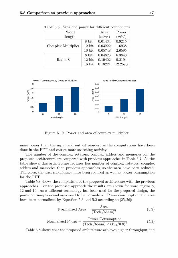
The performance of the complex multipliers and radix-8 butterfly have beenevaluated in terms of power and area. The area and the power for the complexmultiplier and the radix-8 butterfly are described in Table 5.5 for wordlength 8,12 and 16. The bar charts in Figure 5.19 and 5.20 show the power consumptionand area for the complex multiplier and the radix-8 butterfly, respectively. Table5.5 shows the trade off between performance and wordlength. Power consumptionand area increase with the wordlength.
5.8 Comparison to previous approaches
Table 5.6 and bar charts in Figure 5.21 show the performance of the proposedarchitecture in account of power consumption and area. Figure 5.21 shows thepower and area for the FFT and for the input and output reorder. The blue colorof the bars show the power and area for the FFT and the brown color shows thearea and power consumption of the input and output reorder. The FFT consumes
5.8 Comparison to previous approaches 47
Table 5.5: Area and power for different componentsWord Area Powerlength (mm2) (mW )
Complex Multiplier8 bit 0.01434 0.921512 bit 0.03222 1.693816 bit 0.05748 2.6595
Radix 88 bit 0.04826 6.384312 bit 0.10402 9.219416 bit 0.18221 12.2570
8 12 160
0.5
1
1.5
2
2.5
3
Power Consumption by Complex Multiplier
Wordlength
Po
we
r
8 12 160
0.01
0.02
0.03
0.04
0.05
0.06
0.07
Area for the Complex Multiplier
Wordlength
Are
a(m
m2)
(mW
)
Figure 5.19: Power and area of complex multiplier.
more power than the input and output reorder, as the computations have beendone in the FFT and causes more switching activity.
The number of the complex rotators, complex adders and memories for theproposed architecture are compared with previous approaches in Table 5.7. As thetable shows, this architecture requires less number of complex rotators, complexadders and memories than previous approaches, so the area have been reduced.Therefore, the area capacitance have been reduced as well as power consumptionfor the FFT.
Table 5.8 shows the comparison of the proposed architecture with the previousapproaches. For the proposed approach the results are shown for wordlengths 8,12 and 16. As a different technology has been used for the proposed design, thepower consumption and area need to be normalized. Power consumption and areahave been normalized by Equation 5.3 and 5.2 according to [25,26]:
Normalized Area =Area
(Tech./65nm)2(5.2)
Normalized Power =Power Consumption
(Tech./65nm)× (Vdd/0.8)2(5.3)
Table 5.8 shows that the proposed architecture achieves higher throughput and
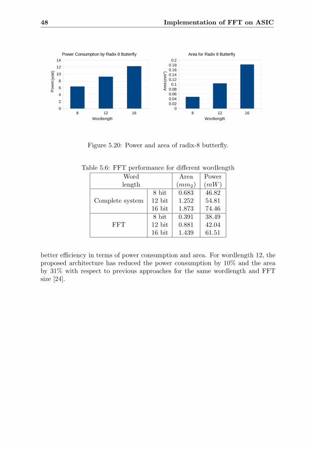
48 Implementation of FFT on ASIC
8 12 160
0.020.040.060.08
0.10.120.140.160.18
0.2
Area for Radix 8 Butterfly
Wordlength
Are
a
8 12 160
2
4
6
8
10
12
14
Power Consumption by Radix 8 Butterfly
Wordlength
Po
we
r (mm
2)
(mW
)
Figure 5.20: Power and area of radix-8 butterfly.
Table 5.6: FFT performance for different wordlengthWord Area Powerlength (mm2) (mW )
Complete system8 bit 0.683 46.8212 bit 1.252 54.8116 bit 1.873 74.46
FFT8 bit 0.391 38.4912 bit 0.881 42.0416 bit 1.439 61.51
better efficiency in terms of power consumption and area. For wordlength 12, theproposed architecture has reduced the power consumption by 10% and the areaby 31% with respect to previous approaches for the same wordlength and FFTsize [24].
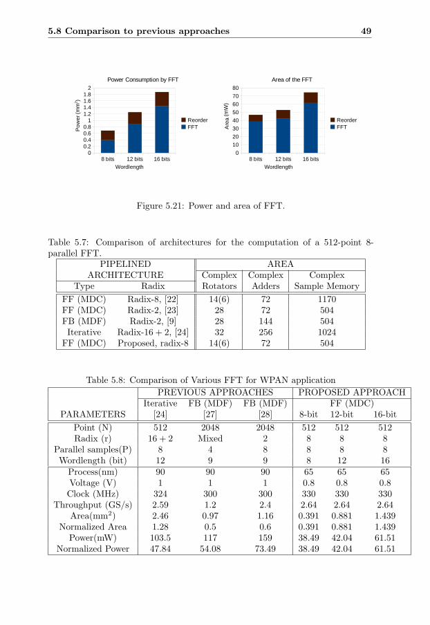
5.8 Comparison to previous approaches 49
8 bits 12 bits 16 bits0
0.20.40.60.8
11.21.41.61.8
2
Power Consumption by FFT
ReorderFFT
Wordlength
Po
we
r
8 bits 12 bits 16 bits0
10
20
30
40
50
60
70
80
Area of the FFT
ReorderFFT
Wordlength
Are
a
(mm
2)
(mW
)
Figure 5.21: Power and area of FFT.
Table 5.7: Comparison of architectures for the computation of a 512-point 8-parallel FFT.
PIPELINED AREAARCHITECTURE Complex Complex Complex
Type Radix Rotators Adders Sample MemoryFF (MDC) Radix-8, [22] 14(6) 72 1170FF (MDC) Radix-2, [23] 28 72 504FB (MDF) Radix-2, [9] 28 144 504Iterative Radix-16 + 2, [24] 32 256 1024
FF (MDC) Proposed, radix-8 14(6) 72 504
Table 5.8: Comparison of Various FFT for WPAN applicationPREVIOUS APPROACHES PROPOSED APPROACH
Iterative FB (MDF) FB (MDF) FF (MDC)PARAMETERS [24] [27] [28] 8-bit 12-bit 16-bit
Point (N) 512 2048 2048 512 512 512Radix (r) 16 + 2 Mixed 2 8 8 8
Parallel samples(P) 8 4 8 8 8 8Wordlength (bit) 12 9 9 8 12 16
Process(nm) 90 90 90 65 65 65Voltage (V) 1 1 1 0.8 0.8 0.8Clock (MHz) 324 300 300 330 330 330
Throughput (GS/s) 2.59 1.2 2.4 2.64 2.64 2.64Area(mm2) 2.46 0.97 1.16 0.391 0.881 1.439
Normalized Area 1.28 0.5 0.6 0.391 0.881 1.439Power(mW) 103.5 117 159 38.49 42.04 61.51
Normalized Power 47.84 54.08 73.49 38.49 42.04 61.51

Chapter 6
Conclusion and Future Work
This chapter discusses conclusion that can be drawn from the previous chaptersand some direction about the future research on this topic.
6.1 Conclusion
Based on the results the following conclusion can be drawn:
• High level model has been done for the standard and BER has been calcu-lated for different level of SNR and wordlength.
• The FFT is parameterizable. This allows to choose wodrlength.
• The FFT has been optimized in order to reduce the area and the powerconsumption. Better results than previous approaches have been obtained.
• Radix-8 and 8 parallel samples reduce the number of hardware elements (20complex multipliers are used).
• Simple control is needed for this architecture.
6.2 Future work
Future work on this topic can be done to improve the results specifically:
• The high level model can be improved by using the ASIC toolbox. For thatcase the model will be more realistic for the hardware point of view.
• The channel model can be more realistic using small scale fading.
• The ASIC can be fabricated to measure the performance on hardware.
• Constant multiplications in the radix 8 butterfly can be simplified.
51

52 Conclusion and Future Work
• A reconfigurable FFT that supports all the modes of this standard can beimplemented.
• Other blocks such as forward error correction and modulation can be imple-mented on ASIC.
Bibliography
[1] I. 802.15.3c, Wireless Medium Access Control (MAC) and Physical Layer(PHY) Specifications for High Rate Wireless Personal Area Networks(WPANs). 2009.
[2] S.-K. S. Yong, P. Xia, and A. Valdes-Garcia, 60 GHz Technology For GbpsWLAN and WPAN. Wiley-IEEE Press, 2010.
[3] L. R. Rabiner and B. Gold, Discrete-time signal processing. Prentice Hall,1975.
[4] A. Oppenheim and R. Schafer, Theory and application of digital signal pro-cessing. Prentice Hall, 1989.
[5] W. W. Smith and J. M. Smith, Handbook of Real-Time Fast Fourier Trans-forms. Wiley-IEEE Press, 1995.
[6] W. Cochran, J. Cooley, D. Favin, H. Helms, R. Kaenel, W. Lang, J. Ma-ling, G.C., D. Nelson, C. Rader, and P. Welch, “What is the fast Fouriertransform?,” Proceedings of the IEEE, vol. 55, pp. 1664–1674, Oct. 1967.
[7] M. Garrido, Efficient hardware architectures for the computation of the FFTand other related signal processing algorithms in real time. PhD thesis, Uni-versidad Politécnica de Madrid, 2009.
[8] E. Swartzlander, W. Young, and S. Joseph, “A radix 4 delay commutatorfor fast Fourier transform processor implementation,” IEEE Journal of Solid-State Circuits, vol. 19, pp. 702–709, Oct 1984.
[9] E. Wold and A. Despain, “Pipeline and Parallel-Pipeline FFT Processorsfor VLSI Implementations,” IEEE Transactions on Computers, vol. C-33,pp. 414–426, May 1984.
[10] A. Despain, “Fourier Transform Computers Using CORDIC Iterations,”IEEE Transactions on Computers, vol. C-23, pp. 993 – 1001, Oct. 1974.
[11] S. He and M. Torkelson, “Design and implementation of a 1024-point pipelineFFT processor,” in Custom Integrated Circuits Conference, 1998. Proceedingsof the IEEE 1998, pp. 131 –134, May 1998.
53
54 Bibliography
[12] M. Sánchez, M. Garrido, M. López Vallejo, J. Grajal, and C. Lopez-Barrio,“Digital channelised receivers on FPGAs platforms,” in Radar Conference,2005 IEEE International, pp. 816 – 821, may 2005.
[13] S. He and M. Torkelson, “Designing pipeline FFT processor for OFDM(de)modulation,” in 1998 URSI International Symposium on Signals, Sys-tems, and Electronics, Sep 1998.
[14] Y. Chang and K. Parhi, “An efficient pipelined FFT architecture,” in IEEETransaction on Circuit and Systems-II: Analog and Digital Signal Processing,June 2003.
[15] S. Johansson, S. He, and P. Nilsson, “Wordlength optimization of a pipelinedFFT processor,” in 42nd Midwest Symposium, Circuits and Systems, vol. 1,Aug.
[16] L. Johnson, “Conflict free memory addressing for dedicated FFT hardware,”in IEEE Transactions Circuits and Systems II: Analog and Digital SignalProcessing, May 1992.
[17] Y. Ma, “An effective memory addressing scheme for FFT processors,” in IEEETransactions on Signal Processing, March 1999.
[18] C. Wang and C. Chang, “A new memory-based FFT processor for VDSLtransceivers,” in IEEE International Symposium on Circuits and Systems,May 2001.
[19] A. Batra, J. Balakrishnan, G. R. Aiello, J. R. Foerster, and A. Dabak, “Designof a multiband OFDM system for realistic UWB channel environment,” inIEEE Transactions on Microwave Theory and Techniques, Sept 2004.
[20] J. Lee, H. Lee, S.-I. Cho, and S.-S. Choi, “A high-speed, low-complexityradix-24 FFT processor for MB-OFDM UWB systems,” in IEEE InternationalSymposium on Circuits and Systems, 2006, May 2006.
[21] S.-M. Kim, J.-G. Chung, and K. Parhi, “Low error fixed-width CSD multiplierwith efficient sign extension,” in IEEE Transactions on Circuits and SystemsII: Analog and Digital Signal Processing, Dec 2003.
[22] M. Sánchez, M. Garrido, M. López, and J. Grajal, “Implementing FFT-baseddigital channelized receivers on FPGA platforms,” IEEE Transactions onAerospace and Electronic Systems, vol. 44, pp. 1567–1585, Oct 2008.
[23] J. Johnston, “Parallel pipeline fast Fourier transformer,” in IEE Proc. FComm. Radar Signal Process., vol. 130, pp. 564–572, Oct 1983.
[24] S.-J. Huang and S.-G. Chen, “A Green FFT Processor with 2.5-GS/s forIEEE 802.15.3c (WPANs),” in International Conference on Green Circuitsand Systems (ICGCS), pp. 9 –13, June 2010.
Bibliography 55
[25] Y. Chen, Y.-W. Lin, Y.-C. Tsao, and C.-Y. Lee, “A 2.4-Gsample/s DVFSFFT Processor for MIMO OFDM Communication Systems,” IEEE Journalof Solid-State Circuits, vol. 43, pp. 1260–1273, May 2008.
[26] B. Baas, “A low-power, high-performance, 1024-point FFT processor,” IEEEJournal of Solid-State Circuits, vol. 34, pp. 380–387, Mar 1999.
[27] Y. Chen, Y.-C. Tsao, Y.-W. Lin, C.-H. Lin, and C.-Y. Lee, “An Indexed-Scaling Pipelined FFT Processor for OFDM-Based WPAN Applications,”IEEE Transactions on Circuits and Systems II: Express Briefs, vol. 55, pp. 146–150, Feb 2008.
[28] S.-N. Tang, J.-W. Tsai, and T.-Y. Chang, “A 2.4-GS/s FFT Processor forOFDM-Based WPAN Applications,” IEEE Transactions on Circuits and Sys-tems II: Express Briefs, vol. 57, pp. 451 –455, June 2010.
