27 lcd color monitor aoc d2757ph d2757ph/bs service · 27" lcd color monitor aoc d2757ph!...
TRANSCRIPT
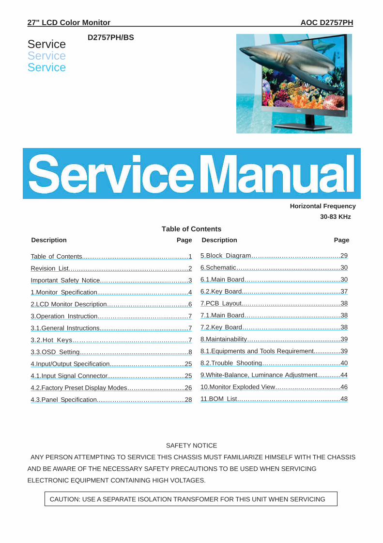
27" LCD Color Monitor AOC D2757PH
Service Service Service
Horizontal Frequency 30-83 KHz
Table of Contents Description Page Description Page
SAFETY NOTICE
ANY PERSON ATTEMPTING TO SERVICE THIS CHASSIS MUST FAMILIARIZE HIMSELF WITH THE CHASSIS
AND BE AWARE OF THE NECESSARY SAFETY PRECAUTIONS TO BE USED WHEN SERVICING
ELECTRONIC EQUIPMENT CONTAINING HIGH VOLTAGES.
Table of Contents.......……..............................……........1
Revision List.…........................................…………........2
Important Safety Notice.……............................……......3
1.Monitor Specification..............................………..........4
2.LCD Monitor Description……………………………......6
3.Operation Instruction…………...............……..............7
3.1.General Instructions...........................…...................7
3.2.Hot Keys…………….…..............……...............7
3.3.OSD Setting…………….…...........................…......8
4.Input/Output Specification............……………............25
4.1.Input Signal Connector............………….................25
4.2.Factory Preset Display Modes…….........................26
4.3.Panel Specification.....………...…………................28
CAUTION: USE A SEPARATE ISOLATION TRANSFOMER FOR THIS UNIT WHEN SERVICING
5.Block Diagram…….........………….................29
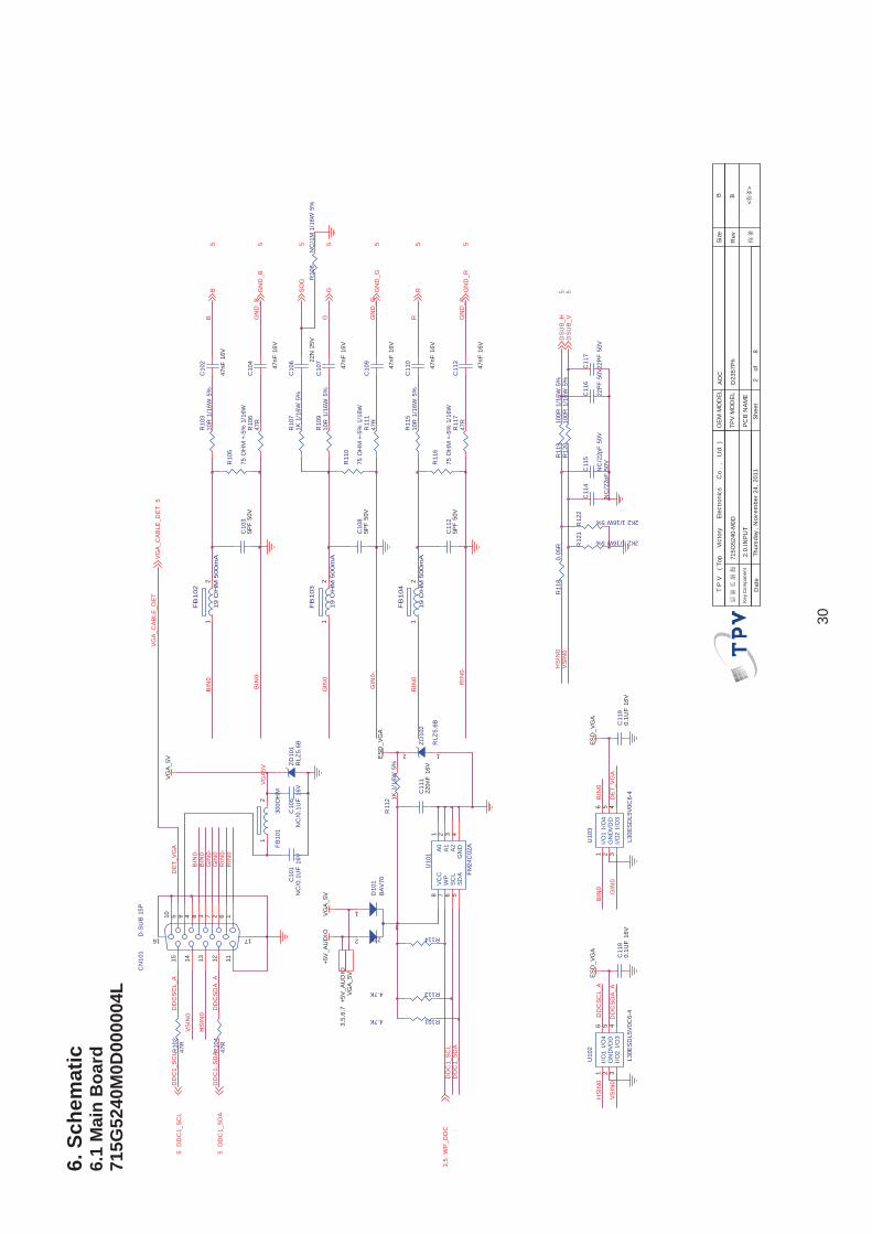
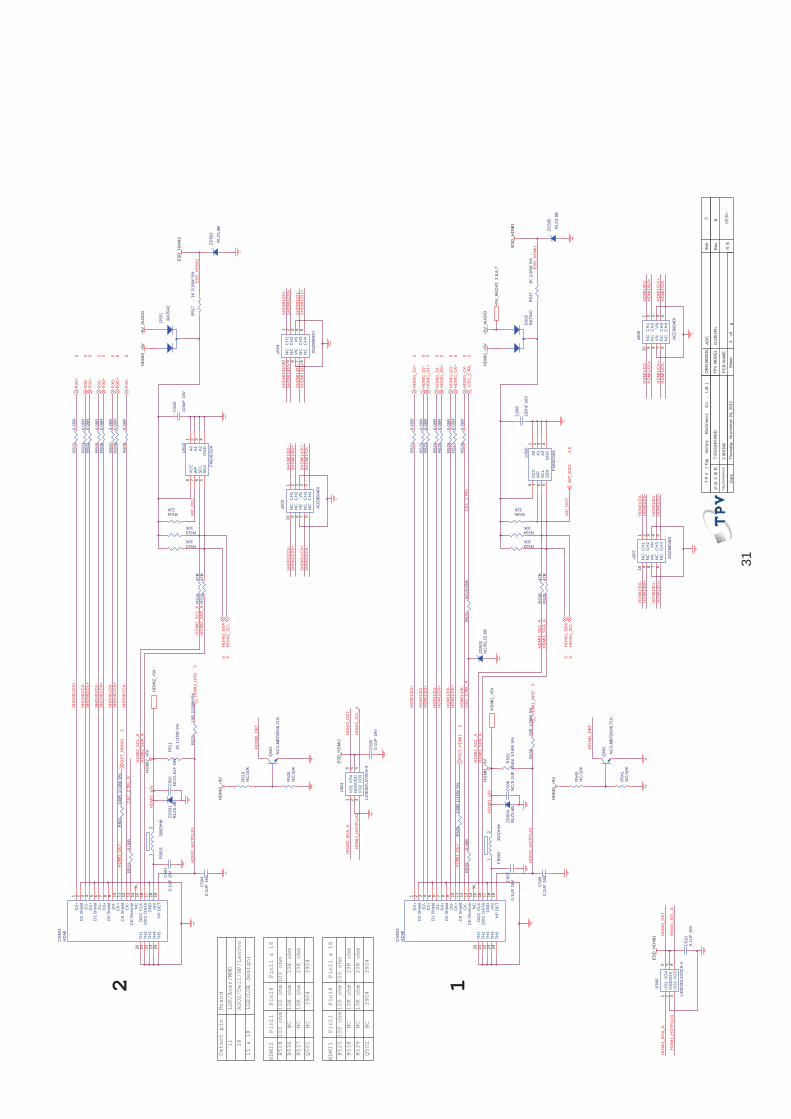
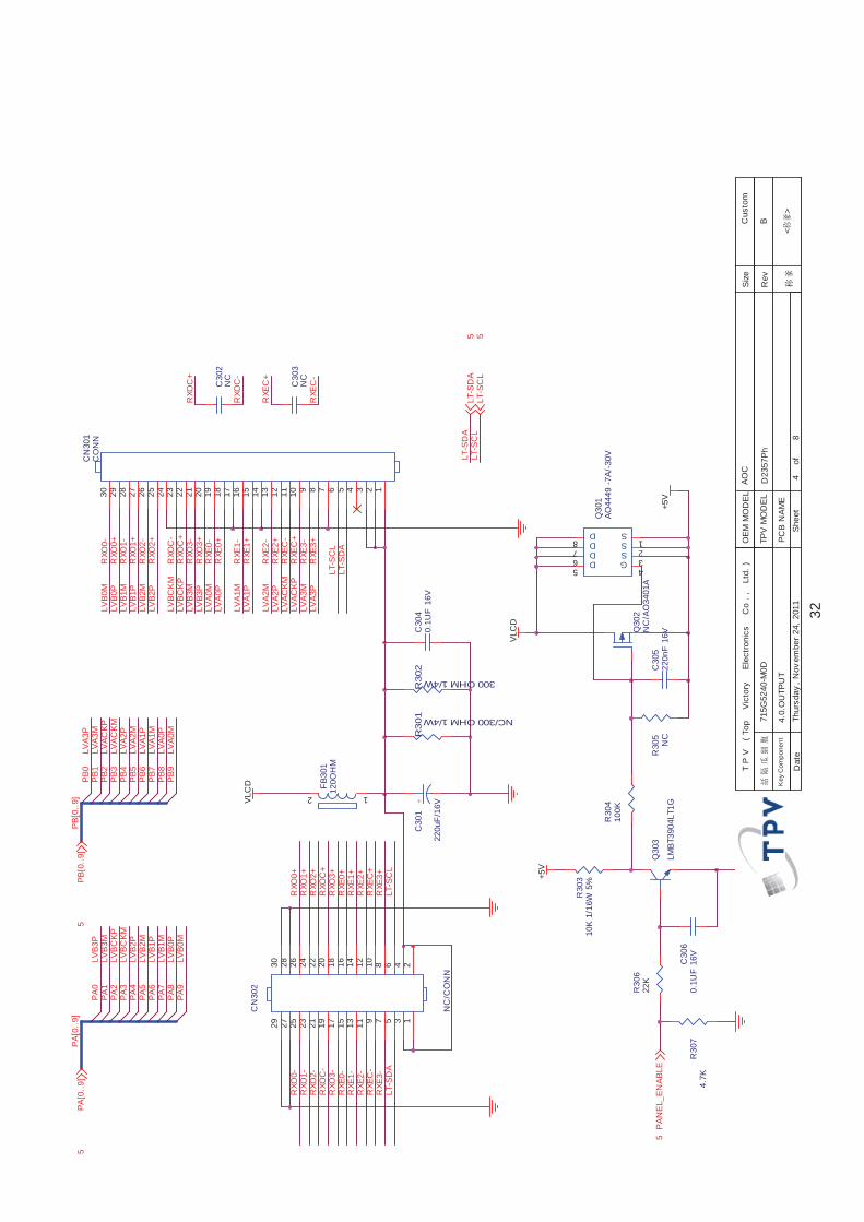
6.Schematic……………........................................30
6.1.Main Board………...........................................30
6.2.Key Board...…….............................................37
7.PCB Layout..………….......................................38
7.1.Main Board………...........................................38
7.2.Key Board…………….....................................38
8.Maintainability……….........................................39
8.1.Equipments and Tools Requirement...............39
8.2.Trouble Shooting………….............................40
9.White-Balance, Luminance Adjustment.............44
10.Monitor Exploded View………..…….…............46
11.BOM List…………………………………...........48
D2757PH/BS
2
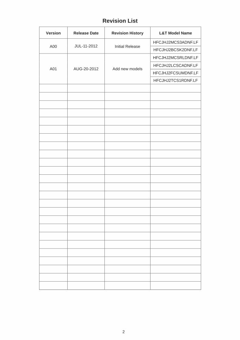
Revision List
Version Release Date Revision History L&T Model Name
A00 JUL-11-2012 Initial ReleaseHFCJHJ2MCS3ADNF.LF
HFCJHJ2BCSK2DNF.LF
A01 AUG-20-2012 Add new models
HFCJHJ2MCSRLDNF.LF
HFCJHJ2LCSCADNF.LF
HFCJHJ2FCSUMDNF.LF
HFCJHJ2TCS1RDNF.LF
3
Important Safety NoticeProper service and repair is important to the safe, reliable operation of all AOC Company Equipment. The service procedures recommended by AOC and described in this service manual are effective methods of performing service operations. Some of these service operations require the use of tools specially designed for the purpose. The special tools should be used when and as recommended.
It is important to note that this manual contains various CAUTIONS and NOTICES which should be carefully read in order to minimize the risk of personal injury to service personnel. The possibility exists that improper service methods may damage the equipment. It is also important to understand that these CAUTIONS and NOTICES ARE NOT EXHAUSTIVE. AOC could not possibly know, evaluate and advise the service trade of all conceivable ways in which service might be done or of the possible hazardous consequences of each way. Consequently, AOC has not undertaken any such broad evaluation. Accordingly, a servicer who uses a service procedure or tool which is not recommended by AOC must first satisfy himself thoroughly that neither his safety nor the safe operation of the equipment will be jeopardized by the service method selected. Hereafter throughout this manual, AOC Company will be referred to as AOC.
WARNING Use of substitute replacement parts, which do not have the same, specified safety characteristics may create shock, fire, or other hazards. Under no circumstances should the original design be modified or altered without written permission from AOC. AOC assumes no liability, express or implied, arising out of any unauthorized modification of design. Servicer assumes all liability. FOR PRODUCTS CONTAINING LASER: DANGER-Invisible laser radiation when open AVOID DIRECT EXPOSURE TO BEAM. CAUTION-Use of controls or adjustments or performance of procedures other than those specified herein may result in hazardous radiation exposure. CAUTION -The use of optical instruments with this product will increase eye hazard. TO ENSURE THE CONTINUED RELIABILITY OF THIS PRODUCT, USE ONLY ORIGINAL MANUFACTURER'S REPLACEMENT PARTS, WHICH ARE LISTED WITH THEIR PART NUMBERS IN THE PARTS LIST SECTION OF THIS SERVICE MANUAL. Take care during handling the LCD module with backlight unit -Must mount the module using mounting holes arranged in four corners. -Do not press on the panel, edge of the frame strongly or electric shock as this will result in damage to the screen. -Do not scratch or press on the panel with any sharp objects, such as pencil or pen as this may result in damage to the panel. -Protect the module from the ESD as it may damage the electronic circuit (C-MOS). -Make certain that treatment person’s body is grounded through wristband. -Do not leave the module in high temperature and in areas of high humidity for a long time. -Avoid contact with water as it may a short circuit within the module. -If the surface of panel becomes dirty, please wipe it off with a soft material. (Cleaning with a dirty or rough cloth may
damage the panel.)
4
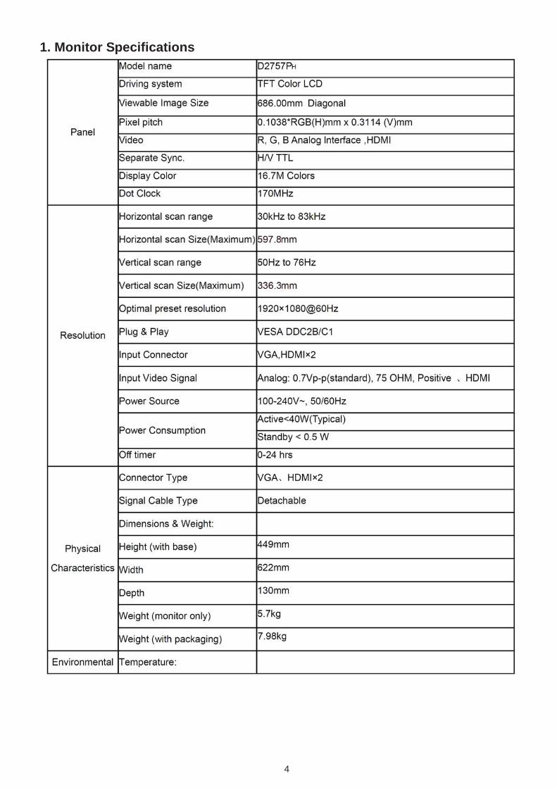
1. Monitor Specifications
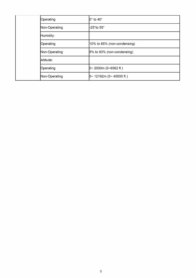
5
6
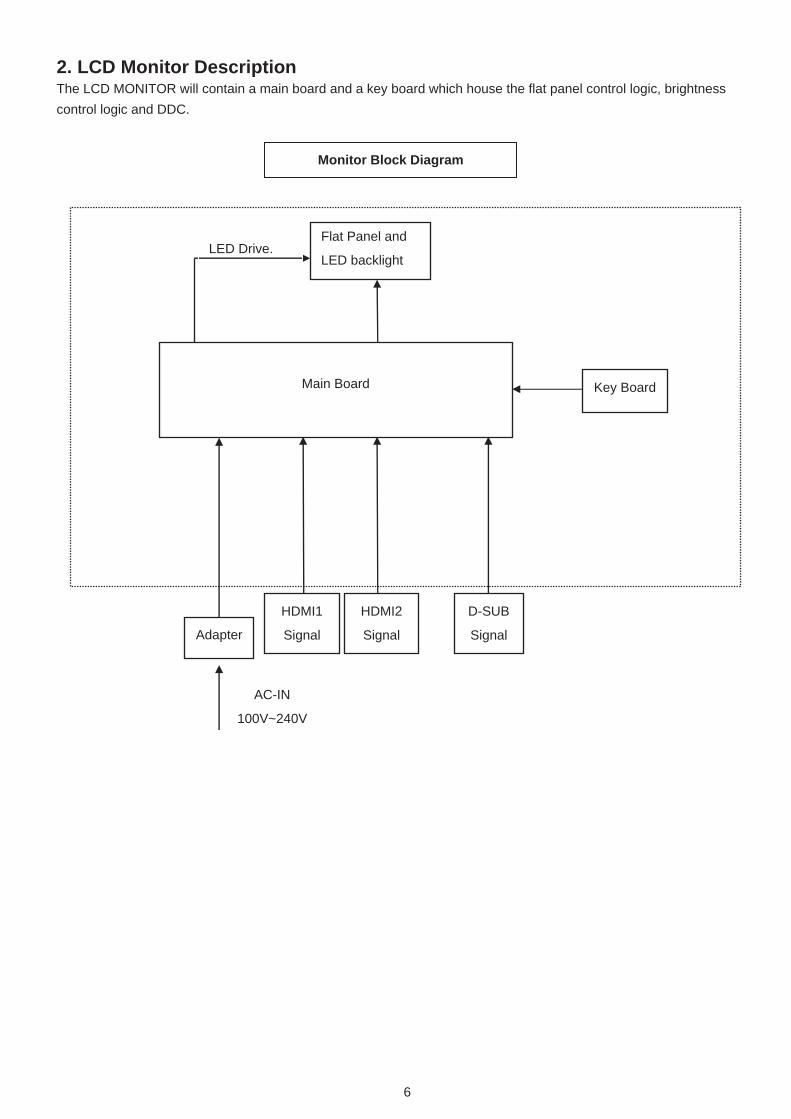
2. LCD Monitor Description The LCD MONITOR will contain a main board and a key board which house the flat panel control logic, brightness control logic and DDC.
Monitor Block Diagram
Flat Panel and
LED backlight
Main Board
Key Board
HDMI2
Signal Adapter
D-SUB
Signal
AC-IN
100V~240V
LED Drive.
HDMI1
Signal
7
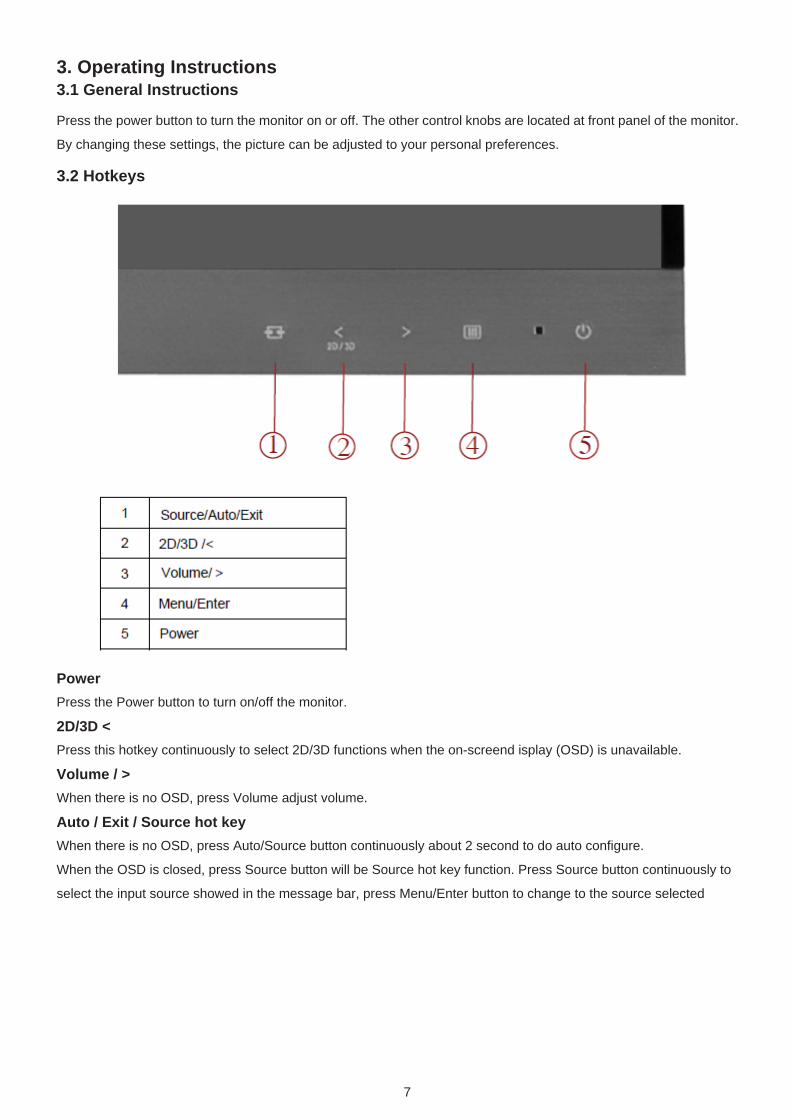
3. Operating Instructions 3.1 General Instructions
Press the power button to turn the monitor on or off. The other control knobs are located at front panel of the monitor.
By changing these settings, the picture can be adjusted to your personal preferences.
3.2 Hotkeys
Power Press the Power button to turn on/off the monitor.
2D/3D < Press this hotkey continuously to select 2D/3D functions when the on-screend isplay (OSD) is unavailable.
Volume / > When there is no OSD, press Volume adjust volume.
Auto / Exit / Source hot key When there is no OSD, press Auto/Source button continuously about 2 second to do auto configure.
When the OSD is closed, press Source button will be Source hot key function. Press Source button continuously to
select the input source showed in the message bar, press Menu/Enter button to change to the source selected
8
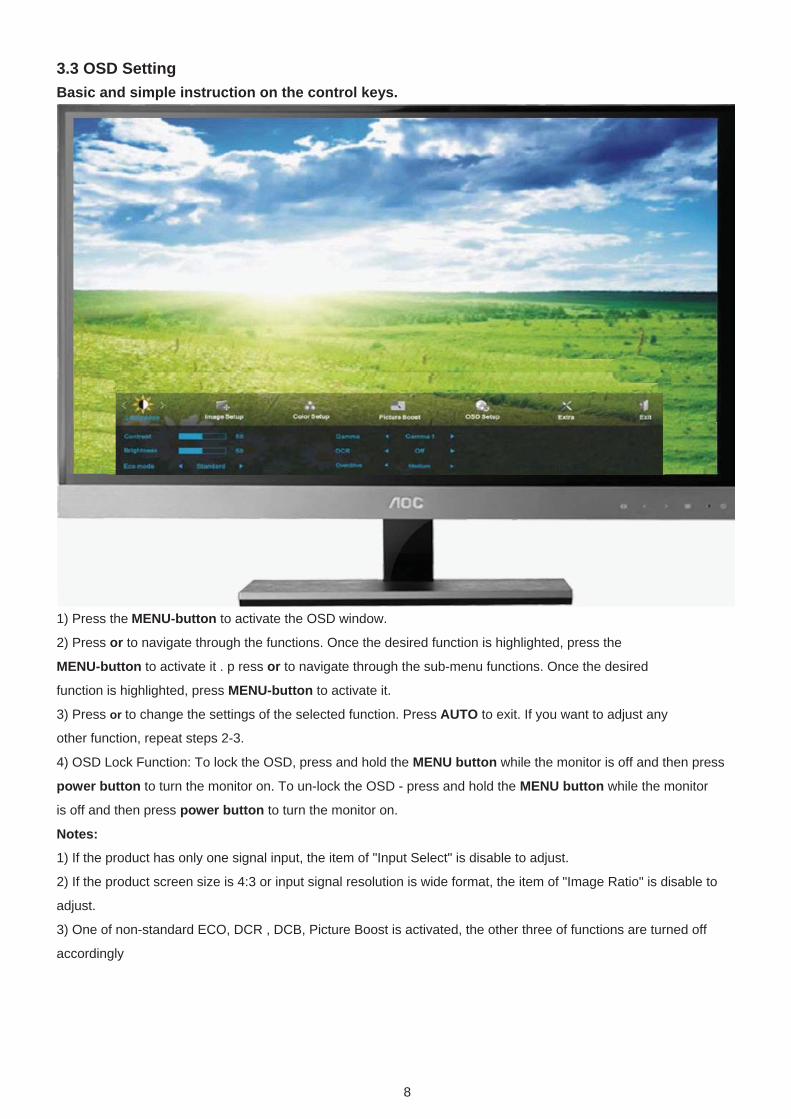
3.3 OSD Setting Basic and simple instruction on the control keys.
1) Press the MENU-button to activate the OSD window.
2) Press or to navigate through the functions. Once the desired function is highlighted, press the
MENU-button to activate it . p ress or to navigate through the sub-menu functions. Once the desired
function is highlighted, press MENU-button to activate it.
3) Press or to change the settings of the selected function. Press AUTO to exit. If you want to adjust any
other function, repeat steps 2-3.
4) OSD Lock Function: To lock the OSD, press and hold the MENU button while the monitor is off and then press
power button to turn the monitor on. To un-lock the OSD - press and hold the MENU button while the monitor
is off and then press power button to turn the monitor on.
Notes:
1) If the product has only one signal input, the item of "Input Select" is disable to adjust.
2) If the product screen size is 4:3 or input signal resolution is wide format, the item of "Image Ratio" is disable to
adjust.
3) One of non-standard ECO, DCR , DCB, Picture Boost is activated, the other three of functions are turned off
accordingly
9
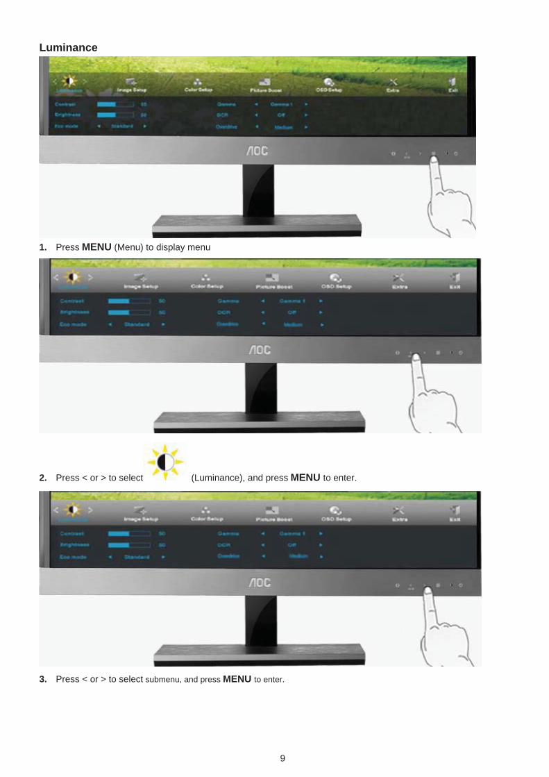
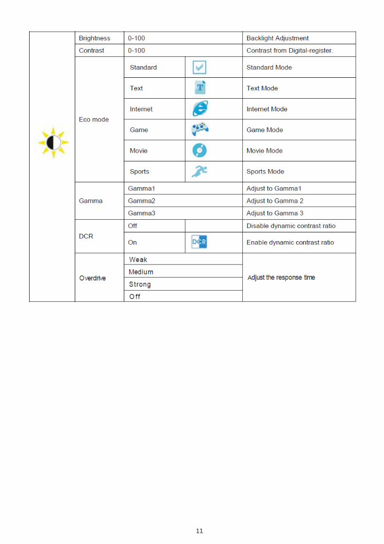
Luminance
1. Press MENU (Menu) to display menu
2. Press < or > to select (Luminance), and press MENU to enter.
3. Press < or > to select submenu, and press MENU to enter.
10
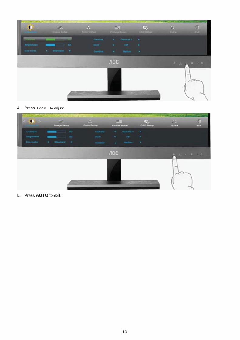
4. Press < or > to adjust.
5. Press AUTO to exit.
11
12
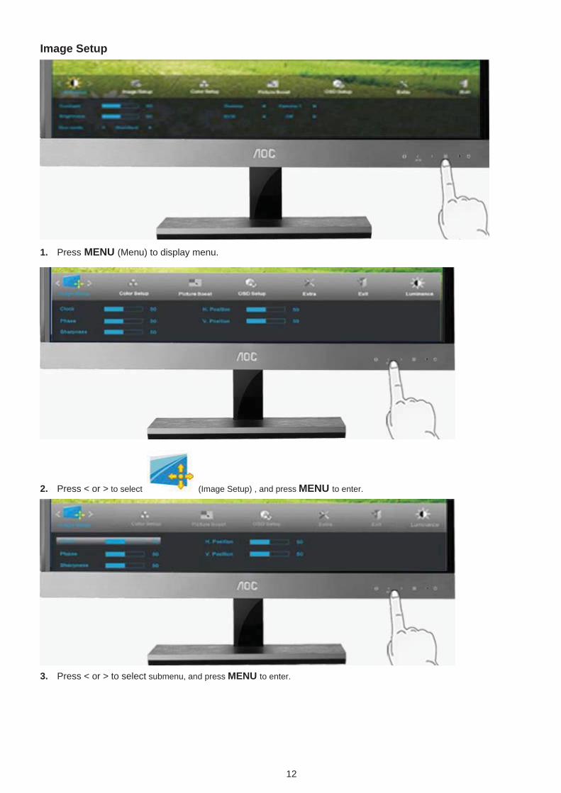
Image Setup
1. Press MENU (Menu) to display menu.
2. Press < or > to select (Image Setup) , and press MENU to enter.
3. Press < or > to select submenu, and press MENU to enter.
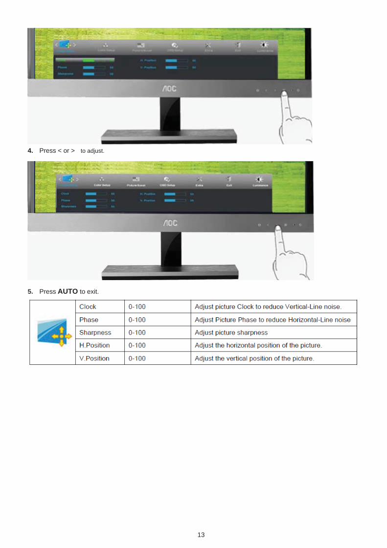
13
4. Press < or > to adjust.
5. Press AUTO to exit.
14
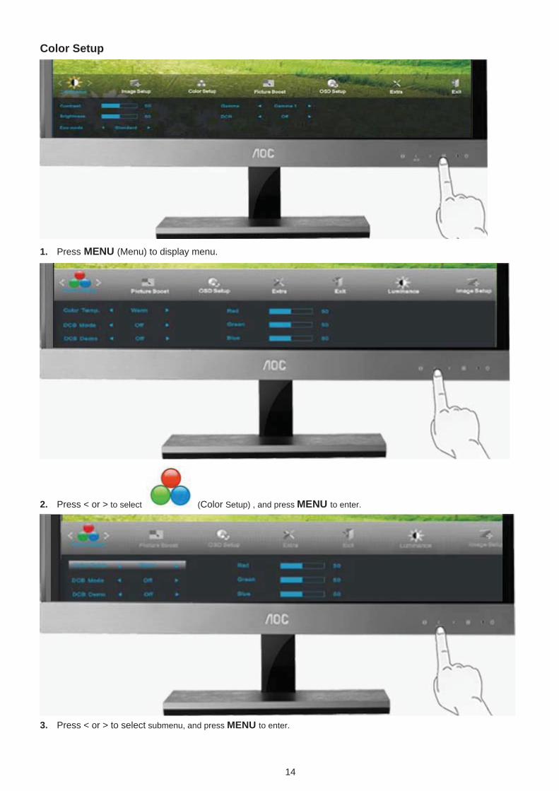
Color Setup
1. Press MENU (Menu) to display menu.
2. Press < or > to select (Color Setup) , and press MENU to enter.
3. Press < or > to select submenu, and press MENU to enter.
15
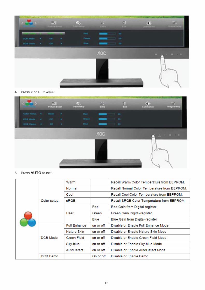
4. Press < or > to adjust.
5. Press AUTO to exit.
16
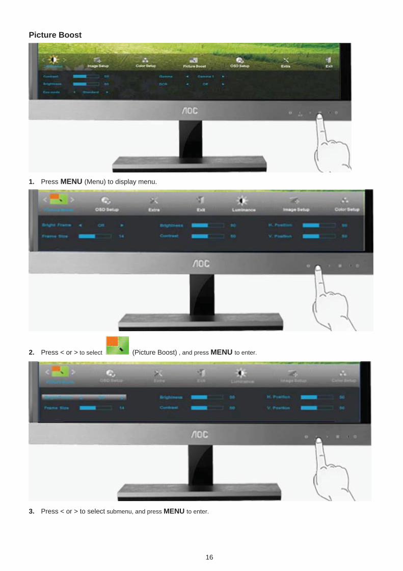
Picture Boost
1. Press MENU (Menu) to display menu.
2. Press < or > to select (Picture Boost) , and press MENU to enter.
3. Press < or > to select submenu, and press MENU to enter.
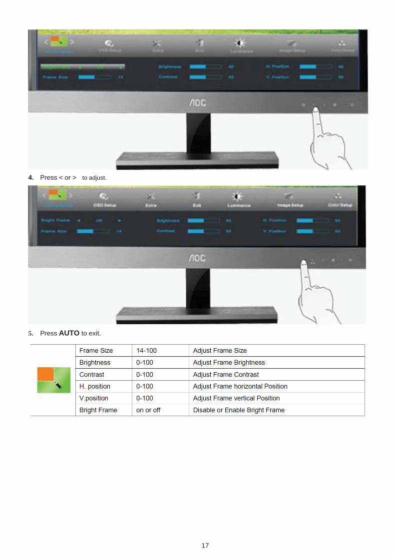
17
4. Press < or > to adjust.
5. Press AUTO to exit.
18
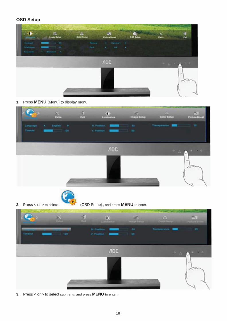
OSD Setup
1. Press MENU (Menu) to display menu.
2. Press < or > to select (OSD Setup) , and press MENU to enter.
3. Press < or > to select submenu, and press MENU to enter.
19
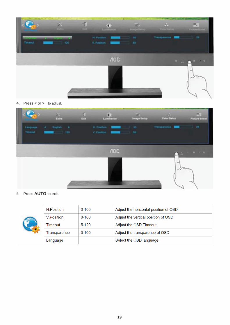
4. Press < or > to adjust.
5. Press AUTO to exit.
20
Extra
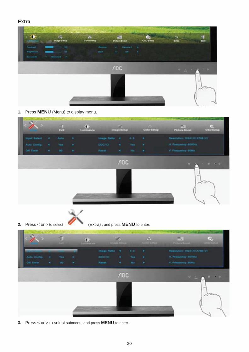
1. Press MENU (Menu) to display menu.
2. Press < or > to select (Extra) , and press MENU to enter.
3. Press < or > to select submenu, and press MENU to enter.
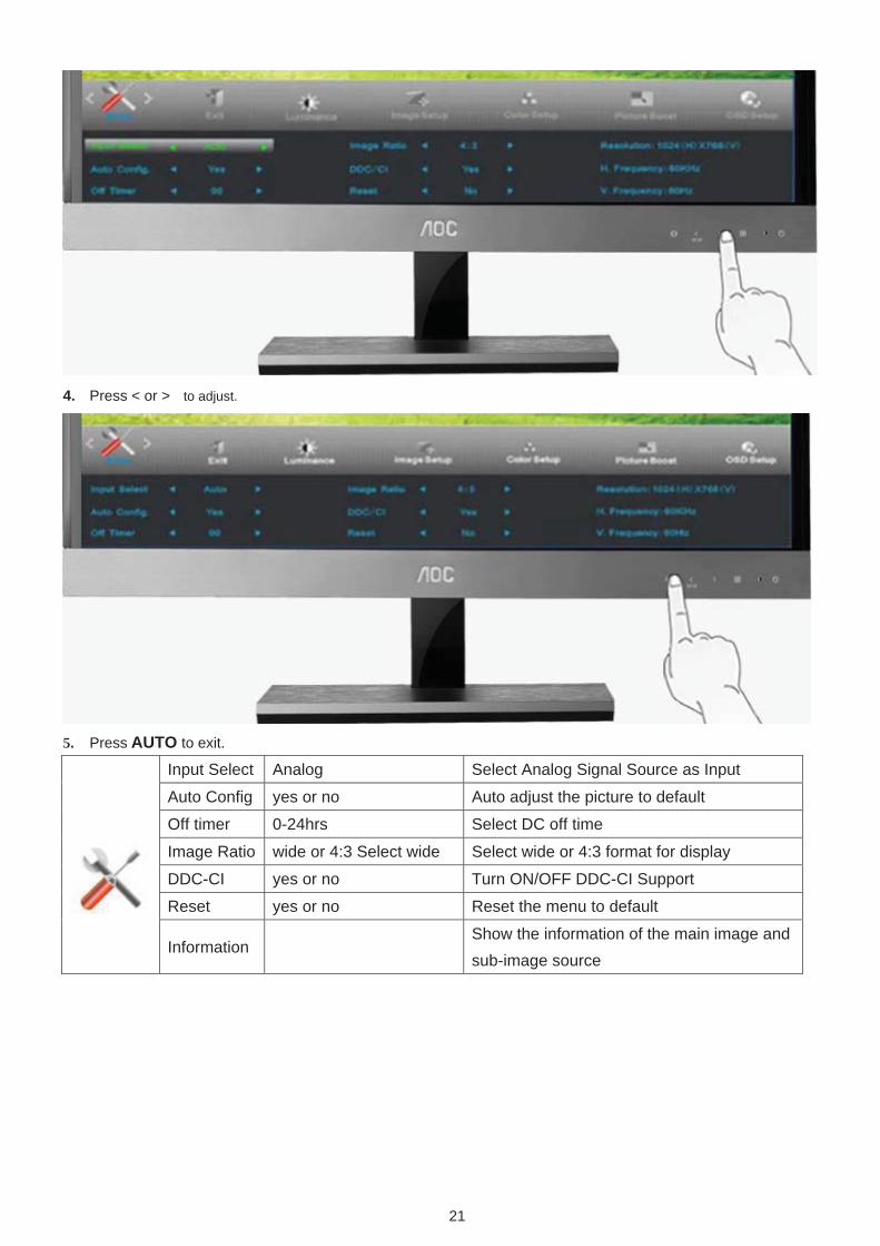
21
4. Press < or > to adjust.
5. Press AUTO to exit.
Input Select Analog Select Analog Signal Source as Input
Auto Config yes or no Auto adjust the picture to default
Off timer 0-24hrs Select DC off time
Image Ratio wide or 4:3 Select wide Select wide or 4:3 format for display
DDC-CI yes or no Turn ON/OFF DDC-CI Support
Reset yes or no Reset the menu to default
Information Show the information of the main image and sub-image source
22
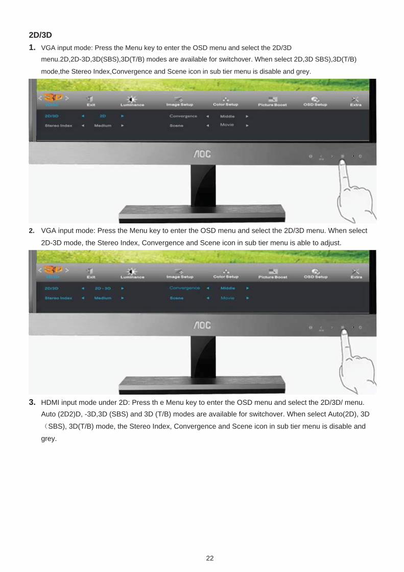
2D/3D1. VGA input mode: Press the Menu key to enter the OSD menu and select the 2D/3D
menu.2D,2D-3D,3D(SBS),3D(T/B) modes are available for switchover. When select 2D,3D SBS),3D(T/B)
mode,the Stereo Index,Convergence and Scene icon in sub tier menu is disable and grey.
2. VGA input mode: Press the Menu key to enter the OSD menu and select the 2D/3D menu. When select
2D-3D mode, the Stereo Index, Convergence and Scene icon in sub tier menu is able to adjust.
3. HDMI input mode under 2D: Press th e Menu key to enter the OSD menu and select the 2D/3D/ menu.
Auto (2D2)D, -3D,3D (SBS) and 3D (T/B) modes are available for switchover. When select Auto(2D), 3D
SBS), 3D(T/B) mode, the Stereo Index, Convergence and Scene icon in sub tier menu is disable and
grey.
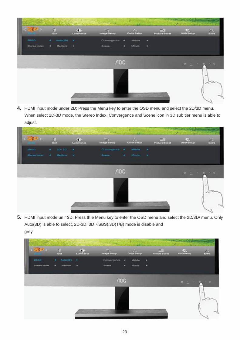
23
4. HDMI input mode under 2D: Press the Menu key to enter the OSD menu and select the 2D/3D menu. When select 2D-3D mode, the Stereo Index, Convergence and Scene icon in 3D sub tier menu is able to
adjust.
5. HDMI input mode un r 3D: Press th e Menu key to enter the OSD menu and select the 2D/3D/ menu. Only Auto(3D) is able to select, 2D-3D, 3D SBS),3D(T/B) mode is disable and
grey
24
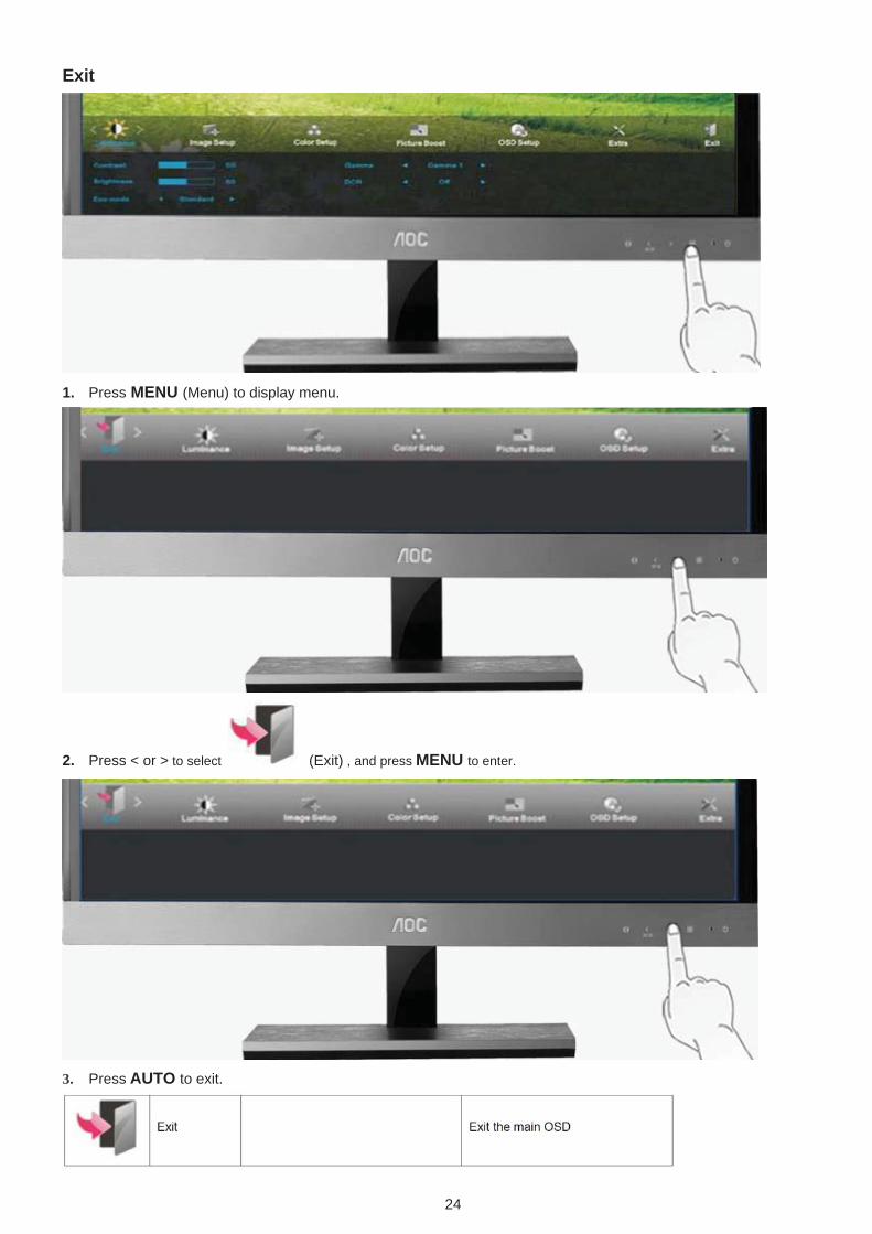
Exit
1. Press MENU (Menu) to display menu.
2. Press < or > to select (Exit) , and press MENU to enter.
3. Press AUTO to exit.
25
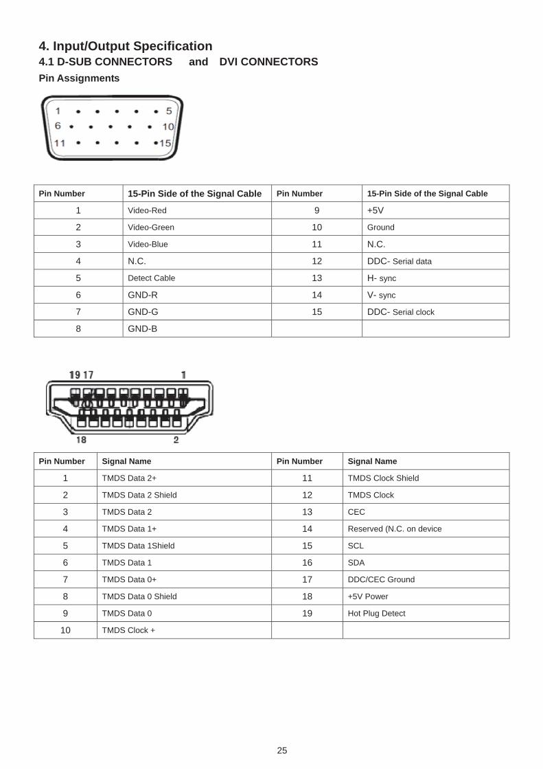
4. Input/Output Specification 4.1 D-SUB CONNECTORS and DVI CONNECTORS Pin Assignments
Pin Number 15-Pin Side of the Signal Cable Pin Number 15-Pin Side of the Signal Cable
1 Video-Red 9 +5V
2 Video-Green 10 Ground
3 Video-Blue 11 N.C.
4 N.C. 12 DDC- Serial data
5 Detect Cable 13 H- sync
6 GND-R 14 V- sync
7 GND-G 15 DDC- Serial clock
8 GND-B
Pin Number Signal Name Pin Number Signal Name
1 TMDS Data 2+ 11 TMDS Clock Shield
2 TMDS Data 2 Shield 12 TMDS Clock
3 TMDS Data 2 13 CEC
4 TMDS Data 1+ 14 Reserved (N.C. on device
5 TMDS Data 1Shield 15 SCL
6 TMDS Data 1 16 SDA
7 TMDS Data 0+ 17 DDC/CEC Ground
8 TMDS Data 0 Shield 18 +5V Power
9 TMDS Data 0 19 Hot Plug Detect
10 TMDS Clock +
26
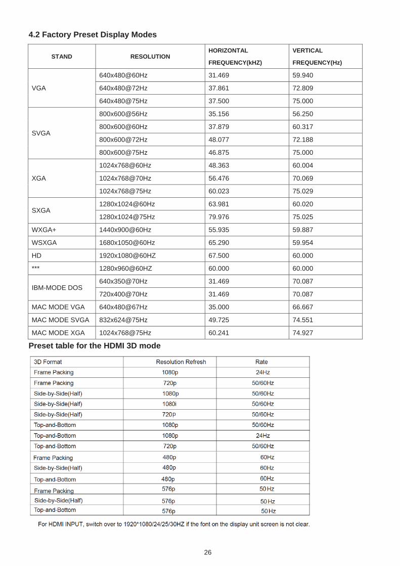
4.2 Factory Preset Display Modes
STAND RESOLUTIONHORIZONTAL
FREQUENCY(kHZ)
VERTICAL
FREQUENCY(Hz)
VGA
640x480@60Hz 31.469 59.940
640x480@72Hz 37.861 72.809
640x480@75Hz 37.500 75.000
SVGA
800x600@56Hz 35.156 56.250
800x600@60Hz 37.879 60.317
800x600@72Hz 48.077 72.188
800x600@75Hz 46.875 75.000
XGA
1024x768@60Hz 48.363 60.004
1024x768@70Hz 56.476 70.069
1024x768@75Hz 60.023 75.029
SXGA 1280x1024@60Hz 63.981 60.020
1280x1024@75Hz 79.976 75.025
WXGA+ 1440x900@60Hz 55.935 59.887
WSXGA 1680x1050@60Hz 65.290 59.954
HD 1920x1080@60HZ 67.500 60.000
*** 1280x960@60HZ 60.000 60.000
IBM-MODE DOS 640x350@70Hz 31.469 70.087
720x400@70Hz 31.469 70.087
MAC MODE VGA 640x480@67Hz 35.000 66.667
MAC MODE SVGA 832x624@75Hz 49.725 74.551
MAC MODE XGA 1024x768@75Hz 60.241 74.927
Preset table for the HDMI 3D mode
27
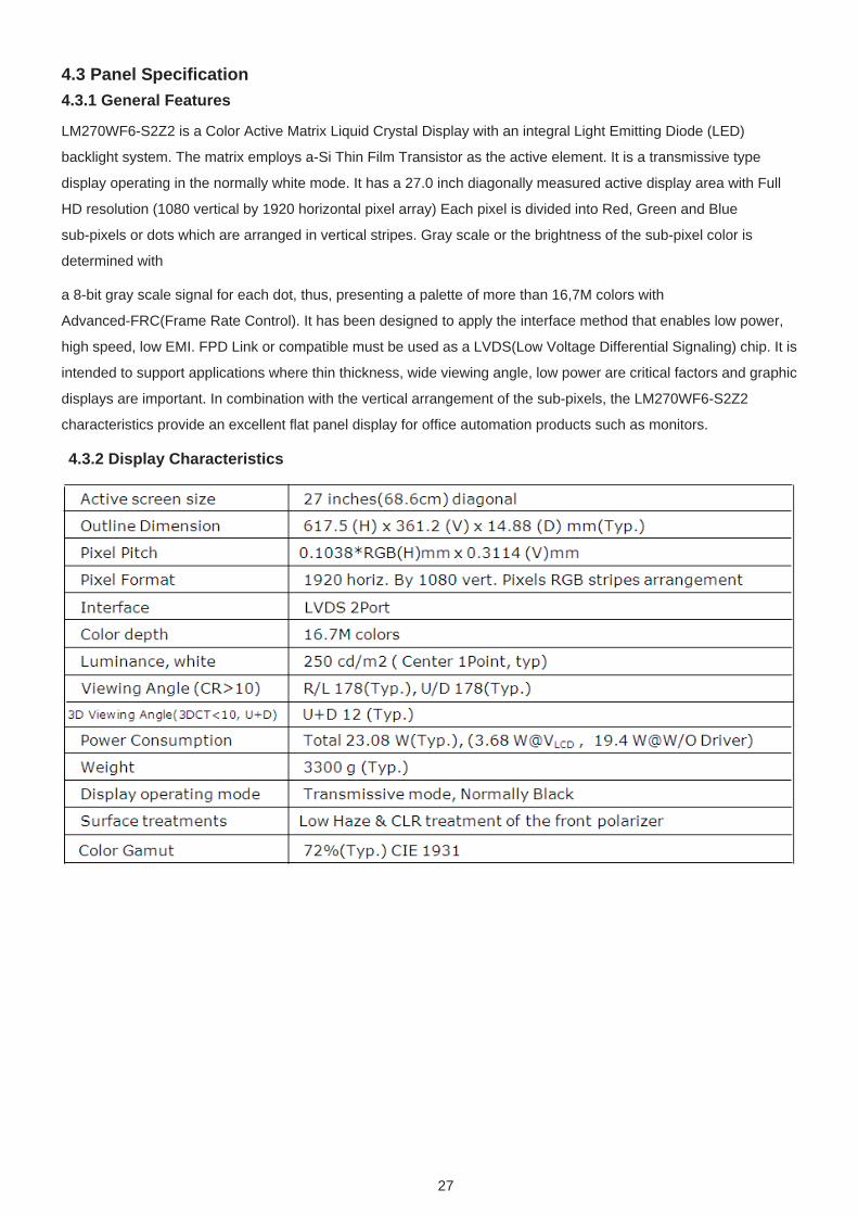
4.3 Panel Specification 4.3.1 General Features
LM270WF6-S2Z2 is a Color Active Matrix Liquid Crystal Display with an integral Light Emitting Diode (LED)
backlight system. The matrix employs a-Si Thin Film Transistor as the active element. It is a transmissive type
display operating in the normally white mode. It has a 27.0 inch diagonally measured active display area with Full
HD resolution (1080 vertical by 1920 horizontal pixel array) Each pixel is divided into Red, Green and Blue
sub-pixels or dots which are arranged in vertical stripes. Gray scale or the brightness of the sub-pixel color is
determined with
a 8-bit gray scale signal for each dot, thus, presenting a palette of more than 16,7M colors with
Advanced-FRC(Frame Rate Control). It has been designed to apply the interface method that enables low power,
high speed, low EMI. FPD Link or compatible must be used as a LVDS(Low Voltage Differential Signaling) chip. It is
intended to support applications where thin thickness, wide viewing angle, low power are critical factors and graphic
displays are important. In combination with the vertical arrangement of the sub-pixels, the LM270WF6-S2Z2
characteristics provide an excellent flat panel display for office automation products such as monitors.
4.3.2 Display Characteristics
28
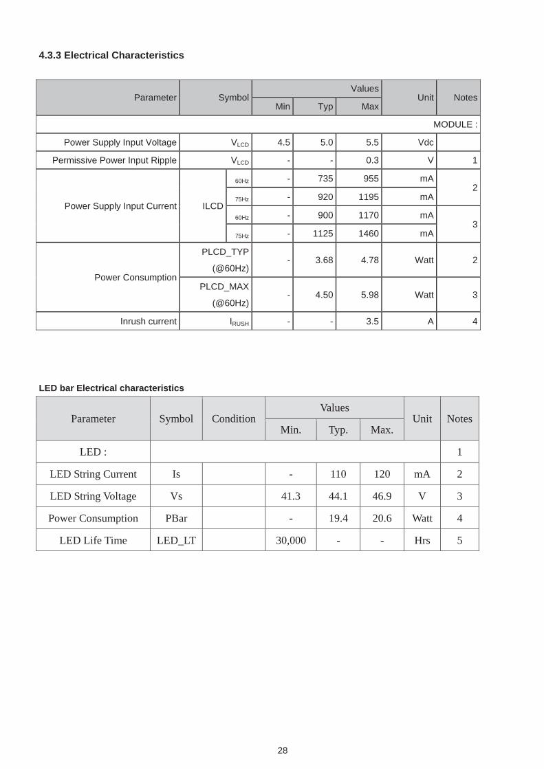
4.3.3 Electrical Characteristics
Parameter SymbolValues
Unit NotesMin Typ Max
MODULE :
Power Supply Input Voltage VLCD 4.5 5.0 5.5 Vdc
Permissive Power Input Ripple VLCD - - 0.3 V 1
Power Supply Input Current ILCD
60Hz - 735 955 mA 2
75Hz - 920 1195 mA
60Hz - 900 1170 mA 3
75Hz - 1125 1460 mA
Power Consumption
PLCD_TYP
(@60Hz)- 3.68 4.78 Watt 2
PLCD_MAX
(@60Hz)- 4.50 5.98 Watt 3
Inrush current IRUSH - - 3.5 A 4
LED bar Electrical characteristics
Parameter Symbol Condition Values
Unit NotesMin. Typ. Max.
LED : 1
LED String Current Is - 110 120 mA 2
LED String Voltage Vs 41.3 44.1 46.9 V 3
Power Consumption PBar - 19.4 20.6 Watt 4
LED Life Time LED_LT 30,000 - - Hrs 5
29
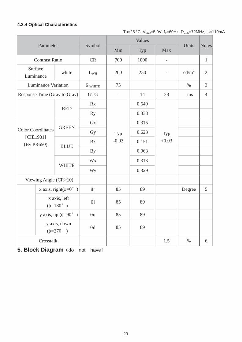
4.3.4 Optical Characteristics Ta=25 °C, VLCD=5.0V, fV=60Hz, DCLK=72MHz, Is=110mA
Parameter Symbol Values
Units NotesMin Typ Max
Contrast Ratio CR 700 1000 - 1
SurfaceLuminance
white LWH 200 250 - cd/m2 2
Luminance Variation WHITE 75 % 3
Response Time (Gray to Gray) GTG - 14 28 ms 4
Color Coordinates [CIE1931]
(By PR650)
REDRx
Typ -0.03
0.640
Typ +0.03
Ry 0.338
GREEN Gx 0.315
Gy 0.623
BLUE Bx 0.151
By 0.063
WHITE Wx 0.313
Wy 0.329
Viewing Angle (CR>10)
x axis, right( =0 ) r 85 89 Degree 5
x axis, left ( =180 )
l 85 89
y axis, up ( =90 ) u 85 89
y axis, down ( =270 )
d 85 89
Crosstalk 1.5 % 6
5. Block Diagram do not have
30
6. S
chem
atic
6.
1 M
ain
Boa
rd
715G
5240
M0D
0000
04L
C10
4
47nF
16V
FB
101
300O
HM
12
C10
5N
C/0
.1U
F 1
6VC
101
NC
/0.1
UF
16V
C10
7
47nF
16V
BIN
0-
RIN
0
BIN
0
C10
9
47nF
16V
BIN
0R
IN0
C11
0
47nF
16V
ES
D_V
GA
U10
2
L30E
SD
L5V0
C6-
4
I/O
11
GN
D2
I/O
23
I/O
34
VD
D5
I/O
46
U10
1
FM
24C
02AA0
1
A12
A23
GN
D4
SDA
5SC
L6
WP
7VC
C8
DD
CSC
L_A
DD
CS
DA
_A
HSI
N0
VS
IN0
GIN
0
B5
C11
3
47nF
16V
GN
D_B
5
SO
G5
DE
T_V
GA
G5
GN
D_G
5
GN
D_R
5
VG
A_5
V
DSU
B_H
5
+5V
_AU
DIO
DSU
B_V
5
DD
C1_
SC
L5
DD
C1_
SD
A5
D10
1B
AV7
0
3
1
2C
106 22
N 2
5V
R11422K
VG
A_C
AB
LE_D
ET
5V
GA
_CA
BLE
_DE
T
R1134.7K
R1014.7K
R10
247
R
R10
447
R
U10
3
L30E
SD
L5V0
C6-
4
I/O
11
GN
D2
I/O
23
I/O
34
VDD
5I/
O4
6
R12
2
2K2 1/16W 5%
R11
910
0R 1
/16W
5%
ZD
101
RLZ
5.6B
VG
A_5
V
VG
A_5
V
OE
M M
OD
EL
Size
Rev
Dat
eS
heet
of
TPV
MO
DEL
PCB
NA
ME
T P
V
( To
p
Vict
ory
E
lect
roni
cs
Co
. ,
Ltd.
)
Key
Com
pone
nt
D23
57Ph
B
AOC
B
28
Thur
sday
, Nov
embe
r 24
, 20
11<
>2.
0.IN
PUT
715G
5240
-M0D
GIN
0
C11
5
NC
/22p
F 5
0VES
D_V
GA
R12
010
0R 1
/16W
5%
R12
1
2K2 1/16W 5%
C11
4
NC
/22p
F 5
0V
RIN
0-
GIN
0-
BIN
0-
WP
_DD
C3,
5
R11
147
R
R10
910
R 1
/16W
5%
R11
747
R
R11
510
R 1
/16W
5% C11
6
22P
F 5
0V
C11
7
22P
F 5
0V
ESD
_VG
A
+5V
_AU
DIO
3,5,
6,7
R11
2 1K 1
/16W
5%
ZD10
2
RLZ
5.6B
12
CN
101
D-S
UB
15P
162738495
111213141510
1716
BIN
0
C11
80.
1UF
16V
GIN
0
GIN
0-
RIN
0-
RIN
0
C11
90.
1UF
16V
FB
103
19 O
HM
500m
A1
2
FB
104
19 O
HM
500m
A1
2
R10
5
75 O
HM
+-5
% 1
/16W
R10
71K
1/1
6W 5
%
C10
35P
F 5
0V
R11
0
75 O
HM
+-5
% 1
/16W
DD
CS
DA
_A
C10
85P
F 5
0V
VGA5
V
DD
CS
CL_
A
R10
647
R
R10
310
R 1
/16W
5%
R11
80.
05R
VSI
N0
HS
IN0
DD
C1_
SD
A
DE
T_VG
A
R11
6
75 O
HM
+-5
% 1
/16W
DD
C1_
SC
L
VS
IN0
HSI
N0
FB
102
19 O
HM
500m
A1
2
C11
25P
F 5
0V
C11
122
0nF
16V
GN
D_R
GN
D_B
GN
D_G
GB
DD
C1_
SDA
DD
C1_
SCL
R10
8N
C/1
M 1
/16W
5%
C10
2
47nF
16V
R5
R
31
OE
M M
OD
EL
Size
Rev
Dat
eSh
eet
of
TPV
MO
DEL
PC
B N
AM
E
T P
V
( To
p
Vict
ory
El
ectro
nics
C
o . ,
L
td.
)
Key
Com
pone
nt
D23
57Ph
B
AOC
C
38
Thur
sday
, N
ovem
ber 2
4, 2
011
<>
3.0H
DM
I
715G
5240
-M0D
U50
1
L30E
SDL5
V0C
6-4
I/O1
1
GN
D2
I/O2
3I/O
34
VD
D5
I/O4
6
U50
6
L30E
SDL5
V0C
6-4
I/O
11
GN
D2
I/O
23
I/O
34
VDD
5I/
O4
6
R51422K
U50
2
FM24
C02
A
A0
1
A1
2
A2
3
GN
D4
SDA
5SC
L6
WP
7VC
C8
R51310K
R50
40.
05R
R51210K
C50
3
220n
F 16
V
R50
50.
05R
R50
80.
05R
R51
1
1K 1
/16W
5%
R50
20.
05R
R51
510
R 1
/16W
5%
R50
60.
05R
R50
90.
05R
R50
70.
05R
C50
40.
1UF
16V
HD
MI2
_+5V
HD
MI2
_+5V
D50
1
BAT
54C
C50
10.
1UF
16V
C50
70.
1UF
16V
WP_
DD
C
SH
DM
I1/D
1-
SH
DM
I1/D
0-
R52
0N
C/1
0K
R51
9N
C/1
0K
Q50
1
NC
/LM
BT3
904L
T1G
HD
MI2
_DET
HD
MI2
_+5V
SH
DM
I1/D
1+
SH
DM
I1/D
0+
SH
DM
I1/D
2+
SH
DM
I1/C
K+
SH
DM
I1/D
2-
SH
DM
I1/C
K-
R51
647
RR
518
47R
HD
MI2
_HO
TPLU
G
R50
110
0R 1
/16W
5%
R52
810
0R 1
/16W
5%
R53
847
RR
539
47R
HD
MI2
_+5V
ESD
_HD
MI2
HD
MI2
_SC
L_A
R53
1N
C/0
.05R
HD
MI2
_SC
L_A
ESD
_HD
MI2
HD
MI2
_SD
A_A
CEC
_CTR
L
HD
MI2
_SD
A_A
HD
MI2
_DE
T
HD
MI2
_SC
L_A
ZD50
1R
LZ5.
6B
ZD50
5
RLZ
5.6B
ZD50
2
RLZ
5.6B
R51
71K
1/1
6W 5
%
R53
71K
1/1
6W 5
%
CEC
_CTR
L_A
ESD
_HD
MI1
ESD
_HD
MI2
R54
1N
C/1
0K
HD
MI1
_DET
R54
0N
C/1
0K
HD
MI1
_+5V
Q50
2
NC
/LM
BT3
904L
T1G
C50
2N
C/0
.1U
F 1
6V
3904
Pin11
LGE/Acer/MMD
100 ohm
3904
10K ohm
100 ohm
Pin18
ASUS/Dell/HP/Lenovo
R50
30.
05R
NC
FB50
130
0OH
M
12
FB5
0230
0OH
M
12
R539
NC
LGE(LGE design)
R538
R525
u504
AO
Z880
4DI
CH
11
CH
22
VN3
CH
34
CH
45
NC
6N
C7
VN8
NC
9N
C10
NC
10K ohm
Brand
Pin11 & 18
R508
1
NC
R536
Detect pin
10K ohm
NC
SH
DM
I1/D
0+S
HD
MI1
/D0-
HD
MI1
_DET
R537
HD
MI2
_+5V
HD
MI1
_SC
L_A
10K ohm
NC
HD
MI1
_HO
TPLU
G
SH
DM
I1/D
1+S
HD
MI1
/D1-
SH
DM
I1/D
0-
HD
MI1
_SD
A_A
SH
DM
I1/D
0+
SH
DM
I1/D
1+S
HD
MI1
/D1-
18
10K ohm
Q501
2
10K ohm
Pin11
HDMI211
u503
AOZ
8804
DI
CH
11
CH
22
VN
3
CH
34
CH
45
NC
6N
C7
VN8
NC
9N
C10
100 ohm
Pin18
HDMI1
11 & 18
10K ohm
Pin11 & 18
100 ohm
C50
6N
C/0
.1U
F 16
V
Q502
3904
100 ohm
SHD
MI1
/D2+
SHD
MI1
/D2-
10K ohm
3904
SHD
MI1
/CK
+SH
DM
I1/C
K-
100 ohm
SH
DM
I1/C
K-
SH
DM
I1/D
2-
SH
DM
I1/C
K+
SH
DM
I1/D
2+
RX1
-5
RXC
+5
CN
502
HD
MI
TH1
20
TH2
21
D2+
1
D2
Shie
ld2
D2-
3
D1+
4
D1
Shie
ld5
D1-
6
D0+
7
D0
Shie
ld8
D0-
9
CK+
10
CK
Shi
eld
11
CK
-12
CE
Rem
ote
13
NC
14
DD
C C
LK15
DD
C D
ATA
16
GN
D17
+5V
18
HP
DET
19TH
322
TH4
23
TH5
24
RX2
-5
RX2
+5
RX0
-5
RXC
-5
RX1
+5
RX0
+5
HD
MI2
_DE
T
HD
MI2
_HO
TPLU
G
HD
MI1
_+5V
HD
MI2
_SD
A_A
HD
MI1
_SC
L_A
R53410K
u508
AOZ
8804
DI
CH
11
CH
22
VN
3
CH
34
CH
45
NC
6N
C7
VN8
NC
9N
C10
HD
MI1
/CK+
HD
MI1
/D2-
HD
MI1
/D2+
HD
MI1
/CK-
R53
21K
1/1
6W 5
%
HD
MI1
/D2-
HD
MI1
/CK-
R52
30.
05R
HD
MI1
/D2+
HD
MI1
/CK+
R52
10.
05R
HD
MI1
_SD
A_A
R52
40.
05R
HD
MI1
/CK
-
R52
20.
05R
u507
AO
Z880
4DI
CH
11
CH
22
VN3
CH
34
CH
45
NC
6N
C7
VN
8N
C9
NC
10
U50
5
FM
24C
02AA0
1
A12
A23
GN
D4
SDA
5SC
L6
WP
7VC
C8
HD
MI1
/D0+
HD
MI1
/D1+
HD
MI1
/D1-
HD
MI1
/D0-
R52
50.
05R
HD
MI1
/D1+
HD
MI1
/D0+
HD
MI1
/D0-
HD
MI1
/D1-
R52
60.
05R
R53
00.
05R
R52
70.
05R
HD
MI1
_+5V
DE
T_H
DM
I25
CE
C_C
TRL_
A
+5V_
AUD
IO
HD
MI1
/D2-
HD
MI1
/CK
+
C51
00.
1UF
16V
+5V_
AUD
IO
R52
90.
05R
WP_
DD
C2,
5
HD
MI1
_+5V
HD
MI2
_SD
A5
HD
MI2
_SC
L5
HD
MI1
/D0-
HD
MI1
_DE
T
+5V_
AUD
IO2,
5,6,
7
HD
MI2
_HPD
5
ZD50
4R
LZ5.
6B
HD
MI1
_SC
L5
HD
MI1
_SD
A5
ZD50
3N
C/R
LZ5.
6B
C50
90.
1UF
16V
HD
MI1
_HPD
5
HD
MI1
/D1-
DET
_HD
MI1
5
HD
MI1
_+5V
R53
610
R 1
/16W
5%
CE
C_C
TRL
5
HD
MI1
_D2+
5
ESD
_HD
MI1
HD
MI1
_CK+
5
HD
MI1
_D1-
5
HD
MI1
_D1+
5
HD
MI1
/D0+
HD
MI1
_D0+
5
HD
MI1
_D0-
5
HD
MI1
_D2-
5
HD
MI1
_CK-
5
HD
MI1
_SC
L_A
HD
MI1
_SD
A_A
HD
MI1
/D1+
R53310K
R53522K
C50
8
220n
F 16
VD
502
BAT
54C
ESD
_HD
MI1
HD
MI1
/D2+
HD
MI1
_HO
TPLU
G
WP_
DD
C
C50
50.
1UF
16V
R51
00.
05R
CN
501
HD
MI
TH1
20
TH2
21
D2+
1
D2
Shie
ld2
D2-
3
D1+
4
D1
Shie
ld5
D1-
6
D0+
7
D0
Shie
ld8
D0-
9
CK+
10
CK
Shi
eld
11
CK
-12
CE
Rem
ote
13
NC
14
DD
C C
LK15
DD
C D
ATA
16
GN
D17
+5V
18
HP
DET
19TH
322
TH4
23
TH5
24
32
+C
301
220u
F/16
V
LT-S
DA
5LT
-SC
L5
+5V
C30
60.
1UF
16V
PAN
EL_
EN
ABLE
5
VLC
D
R30
410
0K
Q30
2N
C/A
O34
01A
R30
622
K
Q30
1AO
4449
-7A
/-30
V
S1S2S3G4
D8 D7 D6 D5
+5V
R30
5N
CQ
303
LMBT
3904
LT1G
C30
522
0nF
16V
R30
310
K 1/
16W
5%
R30
74.
7K
C30
40.
1UF
16V
VLC
D
LVA1
MPB
7
LVA2
MPB
5LV
A1P
PB6
LVAC
KMPB
3LV
ACKP
PB2
LVA3
PPB
0LV
A3M
PB1
PB[
0..9
]
LVA2
PPB
4
LVA0
PPB
8
RXO
0-
LVA0
MPB
9
RXO
1-R
XO0+
RXO
2-R
XO1+
RXO
2+
PA6
LVB1
P
PA3
LVBC
KMPA
4LV
B2P
PA0
LVB3
P
PA5
LVB2
M
RXO
C-
PA7
LVB1
M
PA[
0..9
]
PA1
LVB3
M
RXO
C+
PA8
LVB0
P
RXO
3+R
XO3-
RXE
0-R
XE1-
RXE
0+
RXE
C+
RXE
C-
RXE
2+R
XE2-
RXE
1+
RXE
3+R
XE3-
LVA0
PR
XE0+
PA9
LVB0
M
C30
2N
C
PA2
LVBC
KP
FB3
0112
0OH
M
12
C30
3N
C
R30
2
300 OHM 1/4W
CN
301
CO
NN
123456789101112131415161718192021222324252627282930
R301 NC/300 OHM 1/4W
LT-S
DA
LT-S
CL
LT-S
DA
LT-S
CL
LT-S
DA
LT-S
CL
LVB2
MR
XO2-
RXO
3-LV
B3M
RXE
2-LV
A2M
RXO
0-LV
B0M
RXO
1-LV
B1M
LVAC
KM
RXE
C-
RXE
3-LV
A3M
RXO
C+
LVBC
KP
RXE
0-LV
A0M
RXE
1-LV
A1M
RXO
1+LV
B1P
RXO
0+LV
B0P
RXE
2+LV
A2P
LVBC
KM
RXO
C-
RXE
1+LV
A1P
RXO
2+LV
B2P
RXE
C+
LVAC
KP
RXO
3+LV
B3P
RXO
C-
RXE
3+LV
A3P
RXE
C+
RXE
C-
RXO
C+
CN
302
NC
/CO
NN
24681012141618202224262830
1357911131517192123252729
PA[0
..9]
5
OEM
MO
DEL
Size
Rev
Dat
eSh
eet
of
TPV
MO
DE
L
PCB
NAM
E
T P
V
( Top
V
icto
ry
Ele
ctro
nics
C
o . ,
Lt
d. )
Key
Com
pone
nt
D23
57Ph
B
AOC
Cus
tom
48
Thur
sday
, Nov
embe
r 24,
201
1<
>4.
0.O
UTP
UT
715G
5240
-M0D
PB[0
..9]
5
33
R47
522
R 1
/16W
5%
R47
822
R 1
/16W
5%
R47
722
R 1
/16W
5%
FB
406
120
OH
M1
2
R47
9
NC
R48
0
10K
1/16
W 5
%
AIN
R7
R45
24.
7KR
454
10K
1/16
W 5
%
on_B
ACKL
IGH
T6
PAN
EL_E
NAB
LE4
VC
CK
DAC
AVD
D33
adj_
BAC
KLI
GH
T6
XTAL
_OU
T
PB7
PB8
PB9
PB2
PB3
PB4
PB5
PB6
PB[0
..9]
4PB
[0..
9]
PB0
PB1
C40
7
10uF
10V
XTAL
_IN
5V_D
ET
USR
D_M
SCL
VCC
3IO
C40
6
10uF
10V
AVD
D_P
LL
LED
_OR
ANG
E
EAR
AVD
D33
AVD
D33
_HD
MI
TSTM
D
USR
D_M
SDA
HD
MI1
_CK
+3
FB
403
120O
HM
12
HD
MI1
_CK
-3
AVD
D3V
_LV
HD
MI1
_SD
A3
HD
MI1
_SC
L3
U40
1
HX6833-A
HD
MI_
RXB
0P8
HD
MI_
RXB
0N9
HD
MI_
RXB
CKP
10
HD
MI_
RXB
CKN
11
HD
MI_
RXA
2P13
BIN
N22
GIN
P25
SOG
IN26
RIN
N27
RIN
P28
HVSS29
HSY
NC
34
VSY
NC
35
DD
CA
_SD
A/R
S23
2_TX
/GPI
O31
36
DD
CA
_SC
L/R
S232
_RX/
GPI
O30
37
SPD
IF/G
PIO
27/IR
_ctr
l_ou
t_1
60
PI10
1
LVA0
N10
0
LVA0
P99
FM
LV2N
/LVA
1N98
FMLV
2P/L
VA1
P97
FMLV
CLK
N/L
VA2N
96
FM
LVC
LKP/
LVA2
P95
FMLV
1N/L
VAC
KN94
FM
LV1P
/LV
ACK
P93
FM
LV0N
/LVA
3N92
FMLV
0P/L
VA3
P91
BMLV
2P/L
VB0
P87
BMLV
CLK
N/L
VB1N
86
BM
LVC
LKP/
LVB1
P85
BM
LV1N
/LVB
2N84
BMLV
1P/L
VB2
P83
BMLV
0N/L
VBC
KN82
BM
LV0P
/LV
BCK
P81
LVB3
N80
DACVCOM/DACVCOM69
AVDD_PLL (3.3V)127
BIN
P23
HD
MI_
RXA
2N14
GIN
N24
BM
LV2N
/LVB
0N88
DACVREF68
TSTM
D10
2
VCC3IO (3.3V)103
EARAVSS3375
SPKR
/SP
KR/S
PKR
74
SPK
L/SP
KL/S
PKL
73
DACAVSS3372
LVB3
P79
HPR
77
HPL
76
XTA
L_IN
128
XTA
L_O
UT
1
VCCK (1.2V)105
DD
CD
B_SC
L/G
PIO
0211
5
VCCK(1.2V)116
VCC3IO (3.3V)118
EXT_
R3
HD
MI_
RXB
2N5
HD
MI_
RXB
2P4
HD
MI_
RXB
1N7
HD
MI_
RXB
1P6
HD
MI_
RXA
1N16
HD
MI_
RXA
1P15
HD
MI_
RXA
0N18
HD
MI_
RXA
0P17
HD
MI_
RXA
CKN
20H
DM
I_R
XAC
KP19
PVD
D2_
EXTC
32
GNDIO/ GNDK (0V)46
GNDIO/ GNDK (0V)57
AVSS_PLL (0V)2
VCC3IO (3.3V)45
AVSS33 (0V)21
VCCK (1.2V)47
GNDIO/ GNDK (0V)104
AVSS3V_LV(0V)/PVSS3V_LV(0V)90
AVDD3V_LV(3.3V)/PVDD3V_LV(3.3V)89
EARAVDD3378
RST
_N12
2
AVDD33_HDMI12
HVDD30
DD
CD
A_SC
L/G
PIO
1412
1D
DC
DA_
SDA/
GPI
O13
120
PVDD1_3331
PVSS1_3333
DACAVDD3367
SAR
0/G
PIO
2012
3
SAR
1/G
PIO
2112
4
SAR
2/G
PIO
2212
5
SAR
3/G
PIO
2312
6
PAD
_RAI
N0B
71PA
D_L
AIN
0B70
SDI
106
CSN
107
SCK
108
SD
O10
9
DD
CD
B_SD
A/G
PIO
0111
4
GNDK/GNDIO (0V)117
USR
D_M
SDA/
GPI
O15
/I2S_
SCK
111
USR
D_M
SCL/
GP
IO16
/I2S_
WS
112
VCC3IO (3.3V)58
VCCK(1.2V)56
GVO
N/G
PIO
40/I
2S_S
CK/
sync
_3d_
out_
061
OEV
/GP
IO41
/I2S_
WS/
sync
_3d_
out_
162
CPV
/GPI
O42
/I2S_
SD0/
sync
_3d_
out_
263
STV
1/G
PIO
43/I2
S_SD
1/sy
nc_3
d_ou
t_3
64
FTP/
GPI
O44
/I2S_
SD2/
sync
_3d_
out_
465
POL/
GPI
O17
/I2S_
SD3/
sync
_3d_
out_
566
GPI
O03
/PW
MB/
/I2S
_SD
2/sy
nc_p
rote
ct48
GPI
O04
/PW
MC
//I2S
_SD
3/sy
s_pw
dn_1
p2v_
en49
PWM
B/G
PIO
10//P
WM
_dbl
51PW
MC
/GPI
O11
/CM
I_3d
_in
52PW
MD
/GPI
O12
/CM
I_3d
_dut
y_in
53G
PIO
24/s
ync_
3d_o
ut_l
54
GPI
O00
/CEC
110
GPI
O05
50
GPI
O06
119
GPI
O07
113
GPI
O31
/RS2
32_T
X/I2
S_S
D0/
PWM
_OU
T_LE
D43
GP
IO30
/RS2
32_R
X/I2
S_S
D1/
PWM
_OU
T_LE
D44
CEC
/GPI
O26
/IR_c
trl_o
ut_0
59
GPI
O02
/SP
DIF
39
GPI
O25
/syn
c_3d
_out
_r55
GPI
O36
//PW
MC
/CM
I_3d
_in
41
GPI
O37
/PW
MD
/CM
I_3d
_dut
y_in
42
GPI
O35
//PW
M_d
bl/P
WM
_B40
GPI
O01
/CEC
/12v
_pw
dn_e
n38
EPAD129
R44
910
0R 1
/16W
5%
R433 NC/10K 1/16W 5%
RXC
-3
FB
404
120
OH
M1
2
RX2
-3
RX2
+3
RXC
+3
RX0
+3
RX1
-3
RX1
+3
RX0
-3
HD
MI2
_SC
L3
HD
MI2
_SD
A3
SCK
CSN
SDI
R42
410
0R 1
/16W
5%
SDO
PA8
PA9
PA3
PA4
PA5
PA6
PA7
PA[0
..9]
4PA
[0..
9]PA
0PA
1PA
2
HVD
D
PVD
D1_
33
RST
_N
R43
9N
C/1
00R
1/1
6W 5
%
GN
D_G
2
B2
GN
D_B
2
GN
D_R
2
SOG
2G
2
C44
7
10uF
10V
R42
50.
05R
R2
R42
80.
05R
DSU
B_H
2
FB
409
120O
HM
12
AIN
L7
DSU
B_V
2
R42
010
0R 1
/16W
5%
DD
C1_
SCL
2
DD
C1_
SDA
2
R48
7N
C/1
00R
1/1
6W 5
%
LED
_GR
N/B
LUE
R48
8N
C/1
00R
1/1
6W 5
%
SPI_
WP#
WP
_DD
C2,
3
R40
110
R
FB
402
120O
HM
12
EE_
WP
FB
401
120O
HM
12
R41
610
0R 1
/16W
5%
VGA_
CAB
LE_D
ET2
R40
439
0R 1
/16W
5%
FB
407
120O
HM
12
SPI_
WP#
IR_I
N
C44
5
220n
F 16
V
FB
405
120O
HM
12
VC
C3.
3
HD
MI1
_HPD
3
HD
MI2
_HPD
3
FB
408
120
OH
M1
2
C44
6
NC
/5pf
F 16
V
DET
_HD
MI2
3
R39
347
R
R39
247
R
VCC
3.3 R
389
4.7K LT
-SD
A4
LT-S
CL
LT-S
CL
4
LT-S
DA
R38
84.
7K
X401
24.5
76M
Hz
C40
220
pFC
401
20pF
AUD
IO_S
D7
DET
_HD
MI1
3
DE
T_H
DM
I13
DE
T_H
DM
I23
R41
70.
05R
AUD
IO_M
UTE
7
Volu
me
7
VCC
3.3
CE
C_C
TRL
3
C41
50.
1UF
16V
PVD
D1_
33A
VDD
_PLL
C43
50.
1UF
16V
C41
30.
1UF
16V
Clo
se to
HR
3
AUDIO OUT
Clo
se to
HR
3
VCC
3.3
C43
3
10uF
10V
AVD
D3V
_LV
VC
C3.
3
R42
10.
05R
VCC
3IO
AUDI
O DAC 3.
3VVC
C3.
3
C44
00.
1UF
16V
Clo
se to
HR
3
AVD
D33
_HD
MI
C43
90.
1UF
16V
EAR
AVD
D33
VCC
3.3
Clo
se to
HR
3
EAR HPONE 3.
3V
VC
C3.
3
C41
10.
1UF
16V
HV
DD
Clo
se to
HR
3
C43
80.
1UF
16V
Clo
se to
HR
3
VCC
3.3
CN
403
NC
/CO
NN
1 2 3 4 5 6 7
8 9
DAC
AVD
D33
CN
401
NC
/CO
NN
1 2 3 4 5 6 7 8
9 10
CN
405
CO
NN1 2 3 4 5 6
7 8
Clo
se to
HR
3
C43
00.
1UF
16V
C43
20.
1UF
16V
VCC
3.3
VC
C3.
3
C44
10.
1UF
16V
C41
70.
1UF
16V
Clo
se to
HR
3
R44
110
0R 1
/16W
5%
R44
310
0R 1
/16W
5%
R44
510
0R 1
/16W
5%
KEY
1KE
Y2
POW
ER_K
EY#
C44
9
10uF
10V
C44
8
10uF
10V
Clo
se to
HR
3
VCC
1D2
C42
3
0.1UF 16V
R45
74.
7K
VCCK
C42
0 0.1UF 16V
R45
84.
7K
VC
CK
C42
2 0.1UF 16V
C42
1 0.1UF 16V
VCC
3.3
RESET
RS
T_N
C40
3
1UF
10V
VCC
3.3
R40
510
K 1
/16W
5%
IR_I
N
LED
_G
R40
31M
OH
M 1
/16W
+/-
5%
DET
_HD
MI1
X1 GROUNG
SHIELDING
VCC
3.3
R43
8N
C/2
7K
D40
2N
C
1
3
2
USER DATA
R46
7N
C/3
K9 +
/-5%
1/1
6WR
468
NC
/3K
9 +/
-5%
1/1
6W
POW
ER
_KE
Y#
C428 NC/100N16V
CN
404
NC
/CO
NN
1234567
C40
510
UF
CN
402
NC
/CO
NN
123456
R46
40.
05R
R46
2N
C
C424 NC/0.1UF 16V
C427 NC/100N16V
D401 NC/RLZ5.6B
C44
2
NC
/100
N 1
6V
LED
_R
LED
_R
TOU
CH
_PO
WE
R
FB41
1
NC
/120
OH
M
12
C425 NC/0.1UF 16V
C426 NC/100N16V
R46
30.
05R
FB4
10
NC
/120
OH
M
12
VCC
3.3
R46
1N
C
VCC
3.3
VCC
3.3
DET
_HD
MI2
KEY
1
R46
9N
C/3
K9 +
/-5%
1/1
6W
KEY
2
VCC
3.3
R41
02K
2 1/
16W
5%
VCC
3.3
R40
9N
C/0
R05
1/1
6W
LED
_GR
N/B
LUE
R41
14.
7K
+5V_
AUD
IO
+5V_
AUD
IO2,
3,6,
7
R41
2N
C/1
00R
1/1
0W 5
%
LED
_RLE
D_G
R41
4N
C/1
00R
1/1
0W 5
%
Q40
1LM
BT3
906L
T1G
+5V_
AUD
IOR
408
0.05
R
R41
50.
05R
LED
_OR
AN
GE
Q40
2LM
BT3
906L
T1G
+5V
_AU
DIO
R41
320
0R
R40
70.
05R
R40
6N
C
C45
0
10uF
10V
SPK
R
SPK
L
R45
64.
7K
R481NC/100K
R482
NC/200K
U40
2
MX2
5L20
26D
M1I
-12G
CS
1
SO2
WP
3
GN
D4
SI
5S
CK
6H
OLD
7V
CC
8
5V_D
ET
+5V_
AUD
IO2,
3,6,
7
AOU
T_L
7
AOU
T_R
7
R459 NC/10K 1/16W 5%
R460 NC/10K 1/16W 5%
R465 15K 1/16W 5%
R466 15K 1/16W 5%
C40
9
220p
F 5
0V
C40
8
220p
F 50
V
D405 RLZ5.6B
12
R40
210
RXT
AL_
IN
XTA
L_O
UT
D404 RLZ5.6B
12
SPI FLASH
D403 RLZ5.6B
12
R48
6N
C/1
0K 1
/16W
5%
OEM
MO
DEL
Size
Rev
Dat
eSh
eet
of
TPV
MO
DEL
PCB
NAM
E
T P
V
( Top
V
icto
ry
Ele
ctro
nics
C
o . ,
L
td. )
Key
Com
pone
nt
B
AOC
Cus
tom
58
Thur
sday
, Nov
embe
r 24
, 20
11<
>5.
0.SC
ALER
715G
5240
-M0D
D23
57Ph
HD
MI1
_D0-
3H
DM
I1_D
0+3
SCK
CS
N
SDO
SDI
R49
010
0R 1
/16W
5%
R48
910
0R 1
/16W
5%
SPK
R
SPK
L
HD
MI1
_D1-
3H
DM
I1_D
1+3
HD
MI1
_D2+
3H
DM
I1_D
2-3
AVD
D33
_HD
MI
+5V_
AUD
IO
EE_W
P USR
D_M
SDA
U40
3
NC
/24L
C02
BT-I/
SN
A0
1
A1
2
A2
3
VSS
4S
DA
5SC
L6
WP
7VC
C8
VCC
3.3
USR
D_M
SCL
R471 NC/4K7 1/16W 5%
C44
3
NC
/220
nF 1
6V
R48
3N
C/1
00R
1/1
6W 5
%
R472 NC/4K7 1/16W 5%
R470 NC/4K7 1/16W 5%
R47
622
R 1
/16W
5%
R48
4N
C/1
00R
1/1
6W 5
%
34
R71
210
K +-
1% 1
/10W
R70
8
53.
6KO
HM
+-1
% 1
/10WC
712
100p
F 5
0VR
707
10R
1/1
0W 5
%
C72
022
PF 5
0V
R71
030
K 1
/16W
C72
22N
2 50
V+C
702
470u
F 1
6V
R71
44.
7K
C71
11u
F 1
6V
L701
10uH
R70
910
0K
L702
10uH
+5V
4
BKL
T-E
N8
BKL
T-V
BR
18
U70
1G
5725
AD
JT11
U
VIN
4
EN
1
LX3
VF
B5
GND2
C71
81u
F 16
V
on_B
AC
KLI
GH
T5
adj_
BAC
KLIG
HT
5Q
701
LMB
T390
4LT1
G
R70
351
K 1
%
R70
511
.5K
1%
L70
322U
H
R70
651
K 1
%
D701
SR
34
12
R71
133
K
C71
310
uF 2
5V
C71
70.
1UF
16V
+C
716
470U
F 1
6V
VC
C3.
3
R70
210
0 O
HM
1/1
0W
+C
704
470u
F 1
6V
+5V
_AU
DIO
2,3,
5,7
C72
9
10uF
10V
C70
910
N 5
0V
C70
6
10N
50V
C71
0
2U2
16V
U70
2G
5725
ADJT
11U
VIN
4
EN
1
LX3
VF
B5
GND2
VCC
1D2
ZD70
1ZM
-PTZ
9.1B
ST 9
.1B
12
D702
SR
34
12
+C
723
150U
F 2
5V
C72
8
10uF
10V
C71
5N
C/1
0uF
25V
+5V
C71
40.
1UF
50V+5
V_A
UD
IO
C72
50.
1UF
50V
+5V
_AU
DIO
+5V
_AU
DIO
2,3,
5,7
R70
451
K 1
%
2010/1
/25
2010
/2/25
C71
90.
1UF
16V
+12V
BKL
T-E
N
FB
701
BE
AD
12
C70
82U
2 16
VC
703
10N
50V
+12V
7,8
R71
310
K 1
/16W
5%
C72
6N
C/1
00N
16V
R71
722
K
R71
610
0R 1
/16W
5%
+5V_
AU
DIO
VC
C3.
3
R71
510
K 1
/16W
5%
C73
0N
C/0
.1U
F50
V
CN
701
JAC
K
3 2 1
C70
7
10N
50V
R70
110
0 O
HM
1/1
0W
Vout=0.6(1+R703/R705)=3.26
ZD
702
NC
/RLZ
6.2B
12
OEM
MO
DE
LS
ize
Rev
Dat
eS
heet
of
TPV
MO
DE
L
PC
B N
AM
E
T P
V
( T
op
Vic
tory
Ele
ctro
nics
Co
. ,
Ltd
. )
Key
Com
pone
nt
e235
7Phz
B
AOC
B
68
Thur
sday
, N
ovem
ber
24, 2
011
<>
6.0.
PO
WER
715G
5240
-M0B
C72
110
0pF
50V
Vout=0.6(1+R704/R706)=1.2
U70
3AP
W70
80KA
ITR
L
VIN
1E
N2
UG
ND
3V
CC
4LX
5
CO
MP
6
FB
7
GN
D8
LX9
C72
41N
50V
VC
C3.
3
35
C61
71U
F 1
0V
C62
30.
1UF
16V
R60
411
0R 1
/10W
5%
+5V
_AU
DIO
R60
211
0R 1
/10W
5%
AO
UT_
L5
R60
6
100R
1/1
6W 5
%V
olum
e5
C630
APA2606NI
R622
1K
750
0OHM
NC
12K
R641
NC
R627
NC
C632
Thernal pad
3K
1U
PAM8007HNR
NC
NC
NC
Yes
R640
R643
R642
33K
0.47U
NC
NC
NC
0.47U
AO
UT_
R5
0OHM
No
NC
R644
R645
0OHM
C631
30K
C64
11U
F 1
0V
R64
6
12K
1% 1
/16W
R647 NC/750R 1/10W 5% R648 NC/750R 1/10W 5%
OEM
MO
DE
LS
ize
Rev
Dat
eS
heet
of
TPV
MO
DE
L
PC
B N
AME
T P
V
( T
op
Vi
ctor
y
Ele
ctro
nics
Co
. ,
Ltd
. )
Key
Com
pone
nt
D23
57P
hB
AO
CC
usto
m
78
Thur
sday
, N
ovem
ber
24,
2011
<>
7.0.
AU
DIO
715G
5240
-M0D
OU
TL
OU
TR
R64
9N
C/3
00 O
HM
+C
631
470U
F 1
6V
R62
5N
C/1
00K
1/16
W 5
%
R61
91K
1/1
6W 5
%
U60
1
APA
2606
NAI
-TR
G
LOUTP1 PGND2 PGND3 LOUTN4 PVDD5 MUTE6 VDD7 LINN8 UVP9 VDC10 VOLUME11 HP_LOUT12
HP_ROUT13
BYPASS14
SE/BTL15
AGC16
RINN17
GND18
SD19
PVDD20
ROUTN21
PGND22
PGND23
ROUTP24
Ther
nal P
ad25
SE
R61
23K
1/1
6W
+
C61
622
0uF
/16V
+
C61
522
0uF
/16V
+5V
_AU
DIO
C60
7
1UF
10V
C60
6
1UF
10V
C61
922
0pF
50V
C62
622
0pF
50V
FB
603
120O
HM
12
FB60
4
120O
HM
12
FB
606
120O
HM
12
C61
122
0pF
50V
FB
605
120O
HM
12
OU
T-R
-
C61
422
0pF
50V
OU
T-R
+O
UT-
L-O
UT-
L+
C61
2N
C/2
20pF
50V
C62
1
NC
/220
pF 5
0V
R61
333
K
VO
L
C61
81U
F 1
0V
C62
2
10uF
10V
+5V_
AU
DIO
VC
C3.
3
C61
01U
F 10
V
C60
810
uF 1
0V
+5V
_AU
DIO
C62
50.
1UF
16V
C63
70.
1UF
50V
C63
40.
1UF
16V
C63
610
uF 2
5V
C62
010
uF 2
5VQ
602
LMB
T390
6LT1
G1
2 3
R63
710
K +
-1%
1/1
0W
+5V
_AU
DIO
R61
40.
05R
U60
2A
PW70
80K
AIT
RL
VIN
1EN
2U
GN
D3
VCC
4LX
5
CO
MP
6
FB
7
GN
D8
LX9
D60
1LL
4148
C63
9N
C/1
N 5
0V
R63
530
K 1
/16W
R63
2N
C/0
R05
1/1
0W
C63
21u
F 2
5V
R63
110
K 1/
16W
5%
Q60
1
LMB
T390
4LT1
G
ZD
601
ZM
-PTZ
9.1B
ST
9.1B
12
C64
02N
2 50
V
+12V
+5V_
AU
DIO
R62
822
K
R63
633
K
C63
010
0pF
50V
C62
91u
F 2
5V
MU
TE-1
C62
80.
1UF
16V
R62
310
K 1
/16W
5%
AUD
IO_M
UTE
5
+12V
ZD
602
NC
/RLZ
6.2B
12
R62
647
0R 1
/16W
5%
C63
3N
C/1
0uF
25V
R62
710
K 1
/16W
5%
+12V
6,8
R62
21K
1/1
6W 5
%
R63
310
0K
R62
4N
C/1
0K1/
16W
R63
4 5
3.6K
OH
M +
-1%
1/1
0W
D602
SR
34
12
C63
80.
1UF
16V
L60
122U
H
+5V_
AU
DIO
C63
522
PF
50V
R611 NC/33K
R617 NC/750R 1/10W 5%
R60
81K
1/1
6W 5
%
R60
91K
1/1
6W 5
%
OU
TL
AIN
L
CN
601
PH
ON
EJA
CK
12354
G-2
C604 6.8nF 50V
FB60
2
120O
HM
12
R60
310
0R 1
/16W
5%
R618 NC/750R 1/10W 5%
C60
30.
47uF
16V
R610 NC/33K
C60
20.
47uF
16V
CN
602
PH
ON
EJA
CK
12354
AIN
R
R60
110
0K
G-1
AIN
R5
OUTR
OUTL
AIN
L5
OU
TR
R62
01K
1/1
6W 5
%
C605 6.8nF 50V
SE
FB6
01
120O
HM
12
C60
90.
47uF
16V
C61
3N
C/0
.47u
F 1
6V
R60
510
K 1
/16W
5%
C60
11u
F 1
6V
R60
7
10K
1/1
6W 5
%
VO
L
D60
3S
R34
12
CN
603
CO
NN1234
56
+12V
6,8
AU
DIO
_SD
5
R62
11K
1/1
6W 5
%
MU
TE-1
+5V
_AU
DIO
R64
530
K O
HM
+-1
% 1
/16W
C62
40.
47uF
16V
C62
7N
C/0
.47u
F 1
6V
36
ISEN
1
ISEN
2
ISEN
4
ISEN
3
+C
801
150U
F 2
5V
ISE
N3
ISE
N2
ISE
N4
ISE
N1
+12V
+12V
6,7
BKLT
-VBR
16
BKLT
-EN
6
D80
1
B310
0B
12
R81
7
7.15K
1%
CN
803
NC
/CO
NN
246
135
R81
5 6
.2KO
HM
+-1
% 1
/10W
CN
802
NC
/CO
NN
1 2 3 4 5 6
OE
M M
OD
ELSi
ze
Rev
Dat
eS
heet
of
TPV
MO
DEL
PCB
NA
ME
T P
V
( To
p
Vict
ory
E
lect
roni
cs
Co
. ,
Ltd.
)
Key
Com
pone
nt
D23
57Ph
B
AOC
B
88
Wed
nesd
ay,
Febr
uary
08,
201
2<
>8.
0.C
ON
VER
T
715G
5240
-M0D
ISEN
2
ISEN
1IS
EN4
ISEN
3
CN
801
CO
NN 1 2 3 4 5 6 7 8 9 10
11 12
VLED
VLE
D
C81
3
NC
C80
82N
2 50
V
C80
62N
2 50
V
R801
10
OH
M 1
/4W
U80
1
OZ
9998
BG
N
ISEN
113
ISEN
214
GN
D15
ISEN
316
ISEN
41
ISE
T2
OVP
3R
T4
EN
A5
ISW
6LD
R7
VREF
8VI
N9
STAT
US
10
SSTC
MP
11
PWM
12
R81
91R
C80
939
0P 5
0V
R81
81R
R80
9
10K
R81
0
0.1R
1%
R80
20
OH
M 1
/4W
R82
01R
R81
430
0K
C80
7
0.47
UF
50V
R82
11R
Q80
1
AOD
482
R80
847
0R
C81
4
1N 5
0VC
816
2.2U
F
C81
2
220N
F 25
V
R81
3
5K1 1
/10W
1%
C80
20.
1UF5
0V
C80
5
1uF
16V
C81
7
1N 5
0V
R80
710
R
R81
6
330K
R805
300K
R80
4
160K
1%
C81
5
0.47
UF
50V
C80
3
0.47
UF
50V
R81
1
0.2oH
M 1
% 1
/4W
R812
100
OH
M 1
/10W
C81
0
NC
R80
6
100K
+C
804
33U
F 10
0V
R80
3
10K
C81
1
100p
F 50
V
L801
47U
H
C81
8
0.47
uF 1
6V
37
6.2
Key
Boa
rd
715G
5638
K0A
0000
04S
5V_L
EDD
ATA
SM_C
LK
SM
_IN
T#R
006
0R05
1/1
6W
ZD00
1U
DZ
SNP
5.6B
12
ZD
002
UD
ZSN
P5.
6B
12
CN
001
CA
BLE
1 2 3 4 5 6
R00
50R
05 1
/16W
CIN
_03
CIN
_07
CIN
_11
5V_L
ED
CIN
_01
+-
R00
74K
7 1
/16W
5%
V3.3
R008
4K
7 1
/16W
5%
OE
M M
OD
EL
Size
Rev
Dat
eS
heet
of
TPV
MO
DEL
PCB
NA
ME
T P
V
( To
p
Vic
tory
E
lect
roni
cs
Co
. ,
Ltd.
)
Key
Com
pone
nt
e943
FwC
AO
C e
943F
wA
3
22
Wed
nesd
ay, M
arch
14,
201
271
5G41
64-K
0C<
>2.
0 To
uch
key
715G
4164
-K0C
-000
-004
0_20
1004
20.D
SN
R00
3
4K7
1/16
W 5
%
R00
410
0R 1
/16W
5%
C00
412
P 50
V
C00
810
0P 5
0V
C00
710
0nF
25V
CIN_01
Dif
fere
ntia
lKE
Y0.
1524
CIN
_05
C00
510
0nF
25V
Differential
C00
610
0nF
25V
GPIO_00
SM
_CLK
U00
1
IT72
30E
FN/B
X
CIN
031
CIN
072
CIN
093
CIN
114
VSHILD5
VBIAS6
AVSS7
AVCC8
DVC
C9
SC
LK10
SD
A11
INT#
12
GPIO013 GPIO114 CIN0015 CIN0116 E-PAD17
CIN
_09
Auto
CIN_03
-
SM
_IN
T#S
M_D
ATA
CIN
_05
GPIO_01
Power
V3.3
V3.3
Menu
+
AC_SHIELDVBIAS
Auto
Power
R001
10K
1/1
6W
5%
C00
312
P 5
0V
CIN
_11
AC
_SH
IELD
CIN
_07
CIN
_09
AUTO
_4K
EY0.
1524
-_2
KEY
0.15
24Orange
Blue
D00
1
2 31
MEN
U_5
KEY
0.15
24+_
3KE
Y0.
1524
R00
2
4K7
1/16
W 5
%
PW
R_1
KEY
0.15
24
GP
IO_0
1G
PIO
_00
TP2
KEY
0.15
24
VB
IAS
MENU
CLK
C01
1
1UF
10VV3
.3SM
_DA
TA
38
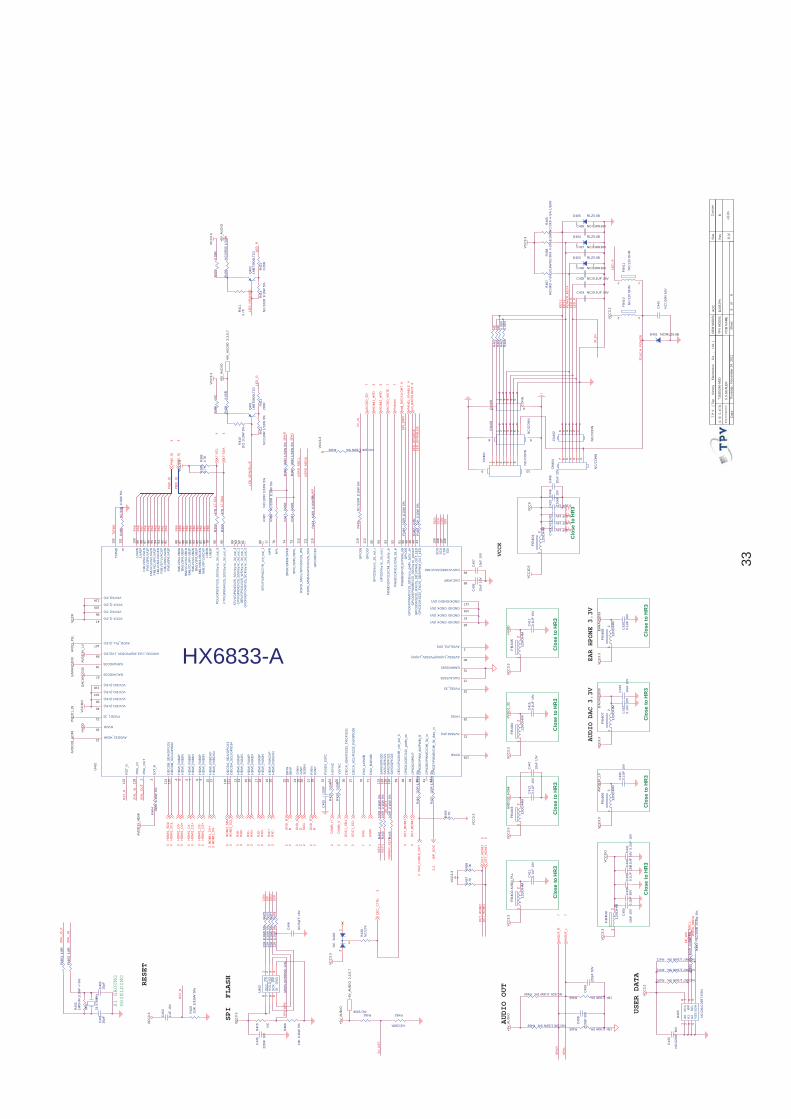
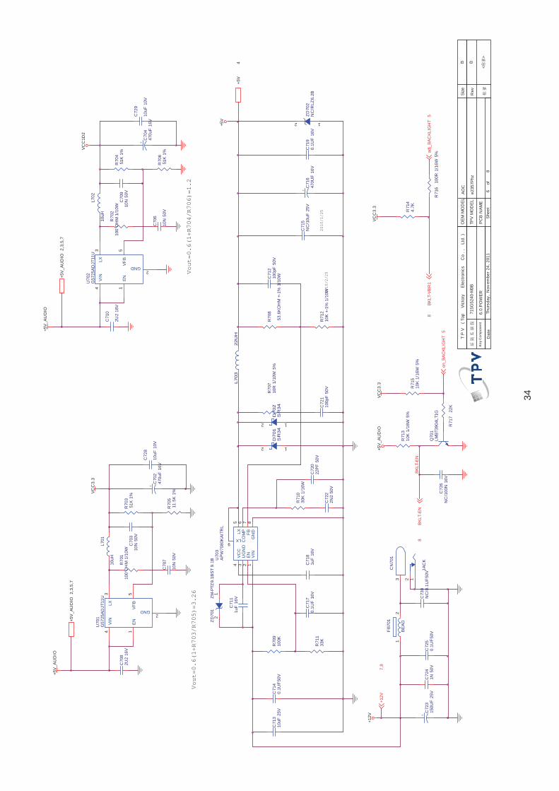
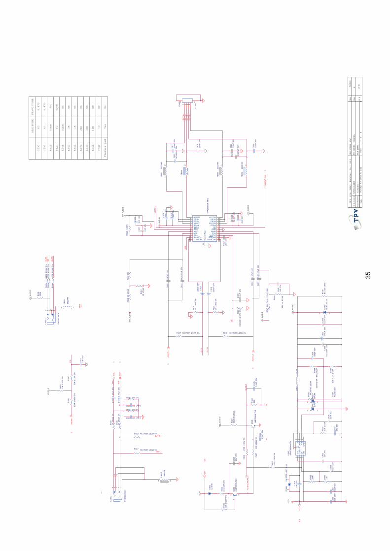
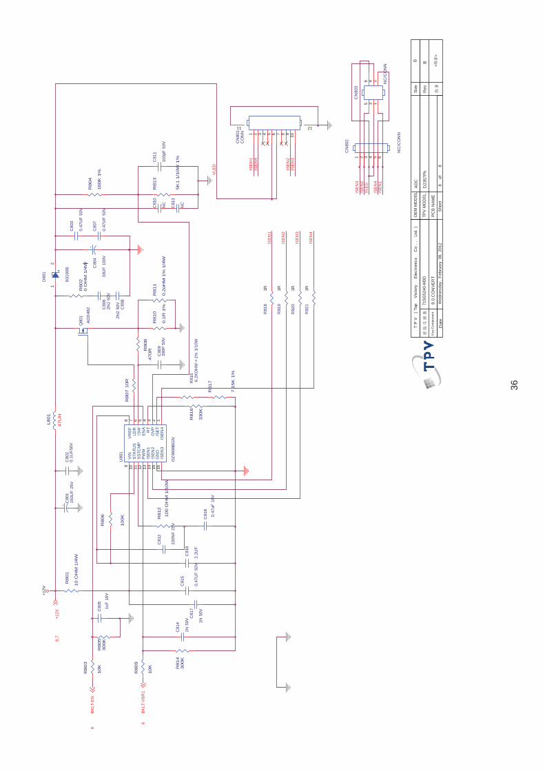
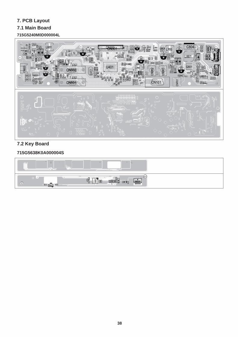
7. PCB Layout 7.1 Main Board 715G5240M0D000004L
ZD3 ZD4
ZD5
C101
C102C103C104
C105
C106C107
C108C109
C110
C111
C112C113
C114
C115
C116
C117
C118
C119
C302 C303 C304
C305
C306
C401
C402
C403
C406
C407
C408
C409
C411
C413
C415
C417
C420
C421
C422
C423
C424
C425
C426
C427
C428
C430 C4
32
C433
C435
C438
C439
C440
C441
C442
C443
C445
C446
C501C5
02
C503C504 C5
05C506 C5
07
C508
C509
C510
C601
C602C603
C604
C605
C606
C607
C608
C609
C610
C611
C612
C613
C614
C617C618
C619
C620
C621
C622
C623
C625
C626
C628
C629
C630
C632
C633
C634
C635
C636C6
37
C638C639
C640
C641
C703
C706
C708
C711
C712
C713
C714
C715
C717 C718
C719
C720
C721C722
C724
C725 C726
C802
C803
C805
C807
C809
C811
C812
C814C815
C816
C817
C818
CN101
CN301
CN40
1CN
402
CN40
3CN
404
CN40
5
CN501
CN502
CN60
1
CN60
2
CN70
1
D101
D402
D501
D502
D602
D701
D801
FB101
FB102
FB103
FB104
FB301
FB40
1
FB402
FB403
FB404
FB405
FB40
6
FB40
7
FB40
8
FB40
9
FB410
FB411
FB50
1FB
502
FB60
1
FB60
2
FB603
FB604
FB605
FB606 FB701
L601 L703
L801
Q301
Q302
Q303
Q401
Q402
Q501
Q502
Q601Q602
Q701
Q801
R101
R102
R103
R104
R105
R106
R107
R108
R109
R110
R111
R112
R113
R114
R115
R116
R117
R118R119
R120
R121
R122
R301
R302
R303
R304
R305
R306
R307
R388
R389
R392
R393
R403
R404
R405
R406
R407
R408
R409
R410
R411
R412
R413
R414
R415
R416
R417
R420
R421
R424
R425
R428
R433
R438
R439
R441R443
R445
R449
R452R454
R456
R457R458
R459
R460
R461
R462
R463R464
R465
R466
R467
R468
R469R470
R471R472
R475
R476
R477
R478
R479
R480
R481
R482
R483R484
R486
R487
R488
R501
R502
R503
R504
R505
R506
R507
R508
R509
R510R511R512
R513
R514
R515
R516
R517
R518
R519
R520
R521
R522
R523
R524
R525
R526
R527
R528
R529
R530R531
R532
R533
R534
R535
R536
R537
R538
R539
R540
R541
R601
R602
R603
R604
R605R606 R6
07
R608
R609
R610
R611
R612
R613
R614
R617
R618
R619
R620
R621
R622R623
R624
R625
R626
R627
R628R631
R632R633
R634
R635R636
R637
R645
R646
R647
R648
R649
R701
R707
R708
R709
R710
R711
R712
R713
R714
R715
R716
R717
R801
R802
R803
R804
R805
R806
R807
R808
R809
R810
R811
R812
R813
R814
R815R816
R817
R818
R819
R820
R821
U101
U102
U103
U402
U403
U501
U502
U505 U506
U601
U602
U701 U7
03
U801
X401
ZD601
ZD70
1
C615
C616 U401
CN302
C624C627
R401
R402
C707
C810
C813
U1
U2
U3
U4
U5
ZD50
2ZD
501
D401D403
D404
D405
D601
ZD101ZD102
ZD503
ZD50
4
ZD50
5ZD60
2
ZD702
C702
C704
C447
CN60
3
CN80
1
CN80
2
C728
C729
CN80
3
R490
R489
C448
C449
C301
U503U504
U508U507
C806
C709
C710
R702U7
02
C808
D702
D603
C405C730
C450
R703
R705
R704
R706
L701
L702
C804C6
31
C716
C723
C801
7.2 Key Board
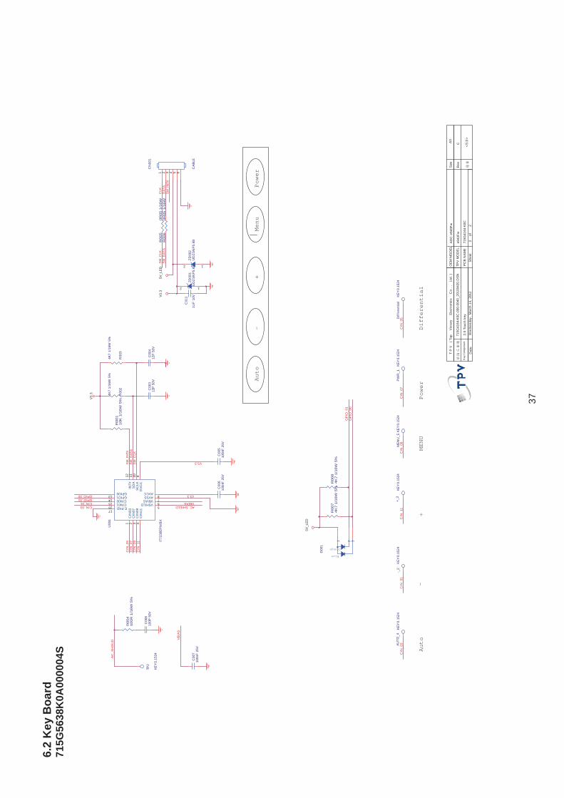
715G5638K0A000004S
PWR_1MENU_5+_3
AUTO_4
-_2CN1 CN2
ZD001ZD00
2
ZD4
ZD5
DIFFERENTIAL
TP2
DIFFERENTIAL1
C003
C004
C005
C006
C007
C008
C011
D001
R001
R002
R003
R004
R005
R006
R007 R008
U001 CN001

39
8. Maintainability8.1 Equipments and Tools Requirement
1. Voltmeter.
2. Oscilloscope.
3. Pattern Generator.
4. DDC Tool with an IBM Compatible Computer.
5. Alignment Tool.
6. LCD Color Analyzer.
7. Service Manual.
8. User Manual.
40
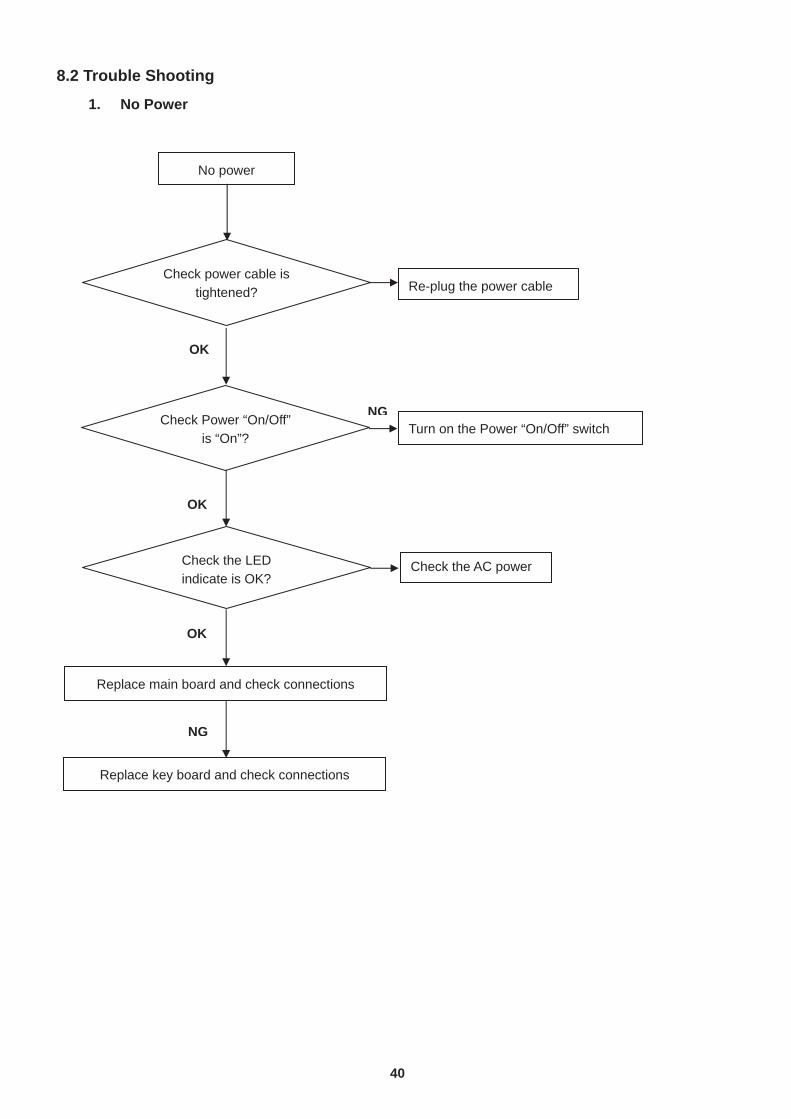
8.2 Trouble Shooting
1. No Power
OK
No power
Check power cable is tightened?
Check Power “On/Off” is “On”?
Re-plug the power cable
Replace key board and check connections
Check the LED indicate is OK?
Check the AC power
Replace main board and check connections
OK
NG
OK
NG
Turn on the Power “On/Off” switch
41
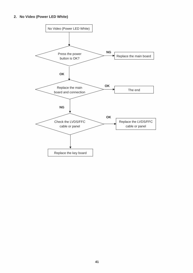
2. No Video (Power LED White)
No Video (Power LED White)
Press the power button is OK?
Check the LVDS/FFC cable or panel
The end
NG
OK
Replace the main board
Replace the LVDS/FFC cable or panel
Replace the key board
NG
Replace the main board and connection
OK
OK
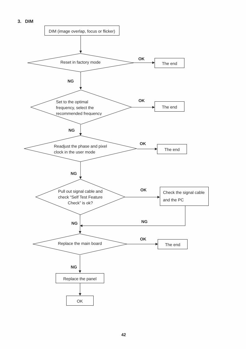
42
3. DIM
OKThe end
OKThe end
OKThe end
DIM (image overlap, focus or flicker)
Reset in factory mode
Set to the optimal frequency, select the recommended frequency
Pull out signal cable andcheck “Self Test Feature
Check” is ok?
Check the signal cable
and the PC
Readjust the phase and pixel clock in the user mode
Replace the main board
Replace the panel
NG
NG
NG
OK
NG
NG
OKThe end
OK
NG
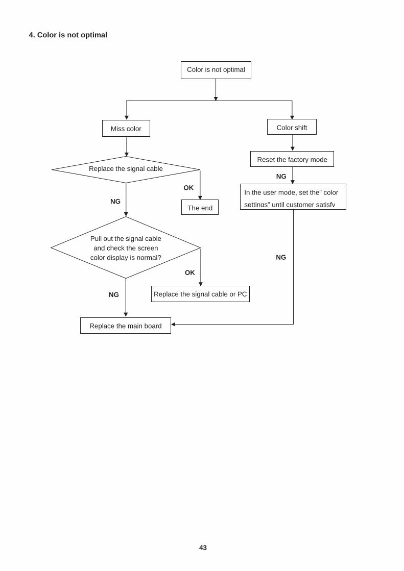
43
4. Color is not optimal
NG
Color is not optimal
Miss color Color shift
Replace the signal cable
Pull out the signal cable and check the screen
color display is normal?
The end
Replace the signal cable or PC
Reset the factory mode
In the user mode, set the” color
settings” until customer satisfy
Replace the main board
NG
OK
NG OK
NG
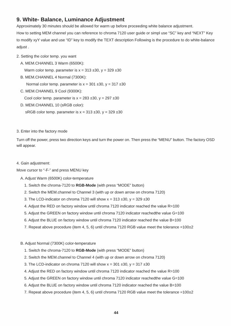
44
9. White- Balance, Luminance Adjustment Approximately 30 minutes should be allowed for warm up before proceeding white balance adjustment.
How to setting MEM channel you can reference to chroma 7120 user guide or simpl use “SC” key and “NEXT” Key
to modify xyY value and use “ID” key to modify the TEXT description Following is the procedure to do white-balance
adjust .
2. Setting the color temp. you want
A. MEM.CHANNEL 3 Warm (6500K):
Warm color temp. parameter is x = 313 ±30, y = 329 ±30
B. MEM.CHANNEL 4 Normal (7300K):
Normal color temp. parameter is x = 301 ±30, y = 317 ±30
C. MEM.CHANNEL 9 Cool (9300K):
Cool color temp. parameter is x = 283 ±30, y = 297 ±30
D. MEM.CHANNEL 10 (sRGB color):
sRGB color temp. parameter is x = 313 ±30, y = 329 ±30
3. Enter into the factory mode
Turn off the power, press two direction keys and turn the power on. Then press the “MENU” button. The factory OSD will appear.
4. Gain adjustment:
Move cursor to “-F-” and press MENU key
A. Adjust Warm (6500K) color-temperature
1. Switch the chroma-7120 to RGB-Mode (with press “MODE” button)
2. Switch the MEM.channel to Channel 3 (with up or down arrow on chroma 7120)
3. The LCD-indicator on chroma 7120 will show x = 313 ±30, y = 329 ±30
4. Adjust the RED on factory window until chroma 7120 indicator reached the value R=100
5. Adjust the GREEN on factory window until chroma 7120 indicator reachedthe value G=100
6. Adjust the BLUE on factory window until chroma 7120 indicator reached the value B=100
7. Repeat above procedure (item 4, 5, 6) until chroma 7120 RGB value meet the tolerance =100±2
B. Adjust Normal (7300K) color-temperature
1. Switch the chroma-7120 to RGB-Mode (with press “MODE” button)
2. Switch the MEM.channel to Channel 4 (with up or down arrow on chroma 7120)
3. The LCD-indicator on chroma 7120 will show x = 301 ±30, y = 317 ±30
4. Adjust the RED on factory window until chroma 7120 indicator reached the value R=100
5. Adjust the GREEN on factory window until chroma 7120 indicator reachedthe value G=100
6. Adjust the BLUE on factory window until chroma 7120 indicator reached the value B=100
7. Repeat above procedure (item 4, 5, 6) until chroma 7120 RGB value meet the tolerance =100±2
45
C. Adjust Cool (9300K) color-temperature
1. Switch the Chroma-7120 to RGB-Mode (with press “MODE” button)
2. Switch the MEM. Channel to Channel 9 (with up or down arrow on chroma 7120)
3. The LCD-indicator on chroma 7120 will show x = 283 ±30, y = 297 ±30
4. Adjust the RED on factory window until chroma 7120 indicator reached the value R=100
5. Adjust the GREEN on factory window until chroma 7120 indicator reached the value G=100
6. Adjust the BLUE on factory window until chroma 7120 indicator reached the value B=100
7. Repeat above procedure (item 4, 5, 6) until chroma 7120 RGB value meet the tolerance =100±2
D. Adjust sRGB color-temperature
1. Switch the chroma-7120 to RGB-Mode (with press “MODE” button)
2. Switch the MEM.channel to Channel 10 (with up or down arrow on chroma 7120)
3. The LCD-indicator on chroma 7120 will show x = 313 ±30, y = 329 ±30
4. Adjust the RED on factory window until chroma 7120 indicator reached the value R=100
5. Adjust the GREEN on factory window until chroma 7120 indicator reachedthe value G=100
6. Adjust the BLUE on factory window until chroma 7120 indicator reached the value B=100
7. Repeat above procedure (item 4, 5, 6) until chroma 7120 RGB value meet the tolerance =100±2
E. Turn the Power-button off to quit from factory mode.
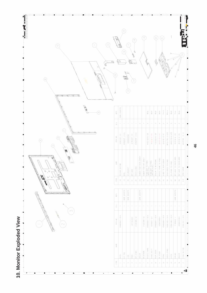
46
10. M
onito
r Exp
lode
d Vi
ew
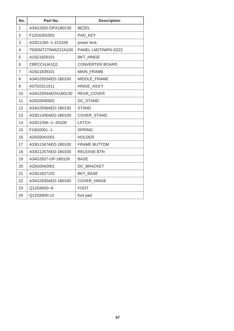
47
No. Part No. Description
1 A34G2932-OPA1B0130 BEZEL
2 F12G6301003 PAD_KEY
3 A33G1260--1-1C0100 power lens
4 750DMT270W6Z21N100 PANEL LM270WF6-S2Z2
5 A15G1826101 BKT_HINGE
6 CBPCCHJA1Q1 CONVERTER BOARD
7 A15G1839101 MAIN_FRAME
8 A34G2933AED-1B0100 MIDDLE_FRAME
9 A37G0311011 HINGE_ASS'Y
10 A34G2934AEDA1B0130 REAR_COVER
11 A20G0040002 DC_STAND
12 A34G2936AED-1B0130 STAND
13 A33G1345AED-1B0100 COVER_STAND
14 A33G1346--1--X0100 LATCH
15 F19G0001--1 SPRING
16 A20G0041001 HOLDER
17 A33G1347AED-1B0100 FRAME BUTTOM
18 A33G1257AED-1B0100 RELEASE BTN
19 A34G2937-OP-1B0100 BASE
20 A20G0042001 DC_BRACKET
21 A15G1827102 BKT_BASE
22 A34G2935AED-1B0100 COVER_HINGE
23 Q12G6600--6 FOOT
24 Q12G6600-12 foot pad
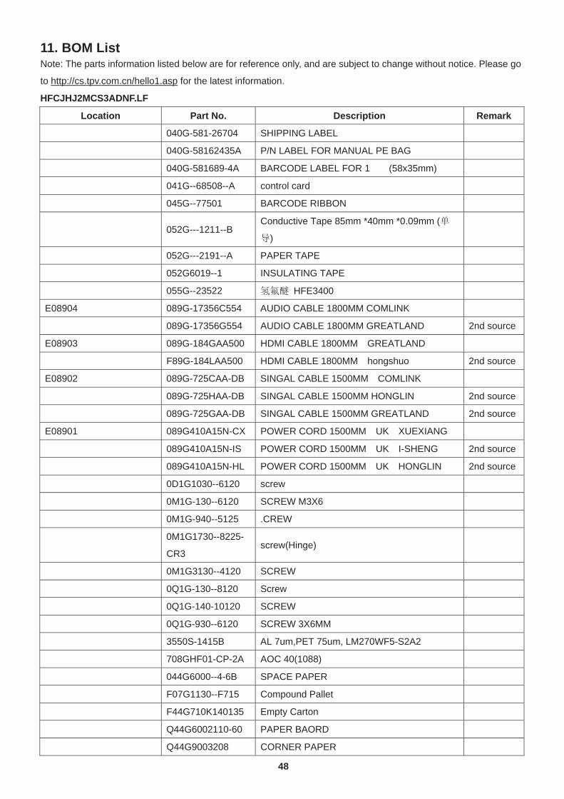
48
11. BOM List Note: The parts information listed below are for reference only, and are subject to change without notice. Please go
to http://cs.tpv.com.cn/hello1.asp for the latest information.
HFCJHJ2MCS3ADNF.LF
Location Part No. Description Remark
040G-581-26704 SHIPPING LABEL
040G-58162435A P/N LABEL FOR MANUAL PE BAG
040G-581689-4A BARCODE LABEL FOR 1 (58x35mm)
041G--68508--A control card
045G--77501 BARCODE RIBBON
052G---1211--B Conductive Tape 85mm *40mm *0.09mm (
)
052G---2191--A PAPER TAPE
052G6019--1 INSULATING TAPE
055G--23522 HFE3400
E08904 089G-17356C554 AUDIO CABLE 1800MM COMLINK
089G-17356G554 AUDIO CABLE 1800MM GREATLAND 2nd source
E08903 089G-184GAA500 HDMI CABLE 1800MM GREATLAND
F89G-184LAA500 HDMI CABLE 1800MM hongshuo 2nd source
E08902 089G-725CAA-DB SINGAL CABLE 1500MM COMLINK
089G-725HAA-DB SINGAL CABLE 1500MM HONGLIN 2nd source
089G-725GAA-DB SINGAL CABLE 1500MM GREATLAND 2nd source
E08901 089G410A15N-CX POWER CORD 1500MM UK XUEXIANG
089G410A15N-IS POWER CORD 1500MM UK I-SHENG 2nd source
089G410A15N-HL POWER CORD 1500MM UK HONGLIN 2nd source
0D1G1030--6120 screw
0M1G-130--6120 SCREW M3X6
0M1G-940--5125 .CREW
0M1G1730--8225-
CR3 screw(Hinge)
0M1G3130--4120 SCREW
0Q1G-130--8120 Screw
0Q1G-140-10120 SCREW
0Q1G-930--6120 SCREW 3X6MM
3550S-1415B AL 7um,PET 75um, LM270WF5-S2A2
708GHF01-CP-2A AOC 40(1088)
044G6000--4-6B SPACE PAPER
F07G1130--F715 Compound Pallet
F44G710K140135 Empty Carton
Q44G6002110-60 PAPER BAORD
Q44G9003208 CORNER PAPER
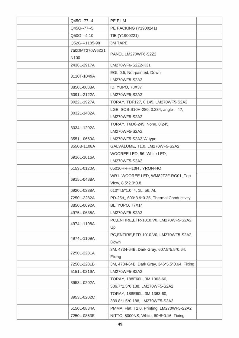
49
Q45G--77--4 PE FILM
Q45G--77--5 PE PACKING (Y1900241)
Q50G---4-10 TIE (Y1900221)
Q52G---1185-98 3M TAPE
750DMT270W6Z21
N100 PANEL LM270WF6-S2Z2
2436L-2917A LM270WF6-S2Z2-K31
3110T-1049A EGI, 0.5, Not-painted, Down,
LM270WF5-S2A2
3850L-0088A ID, YUPO, 78X37
6091L-2122A LM270WF5-S2A2
3022L-1927A TORAY, TDF127, 0.145, LM270WF5-S2A2
3032L-1482A LGE, SOS-S10H-280, 0.284, angle = 4?,
LM270WF5-S2A2
3034L-1202A TORAY, T6D6-245, None, 0.245,
LM270WF5-S2A2
3551L-0669A LM270WF5-S2A2,'A' type
3550B-1108A GALVALUME, T1.0, LM270WF5-S2A2
6916L-1016A WOOREE LED, 56, White LED,
LM270WF5-S2A2
5153L-0120A 05010HR-H10H , YRON-HO
6915L-0438A WR1, WOOREE LED, WM82T2F-RG01, Top
View, 8.5*2.0*0.8
6920L-0238A 610*4.5*1.0, 4, 1L, 56, AL
7250L-2282A PD-25tt,, 609*3.9*0.25, Thermal Conductivity
3850L-0092A BL, YUPO, 77X14
4975L-0635A LM270WF5-S2A2
4974L-1108A PC,ENTIRE,ETR-1010,V0, LM270WF5-S2A2,
Up
4974L-1109A PC,ENTIRE,ETR-1010,V0, LM270WF5-S2A2,
Down
7250L-2281A 3M, 4734-64B, Dark Gray, 607.5*5.5*0.64,
Fixing
7250L-2281B 3M, 4734-64B, Dark Gray, 346*5.5*0.64, Fixing
5151L-0319A LM270WF5-S2A2
3953L-0202A TORAY, 188E60L, 3M 1363-60,
586.7*1.5*0.188, LM270WF5-S2A2
3953L-0202C TORAY, 188E60L, 3M 1363-60,
339.8*1.5*0.188, LM270WF5-S2A2
5150L-0834A PMMA, Flat, T2.0, Printing, LM270WF5-S2A2
7250L-0853E NITTO, 5000NS, White, 60*8*0.16, Fixing
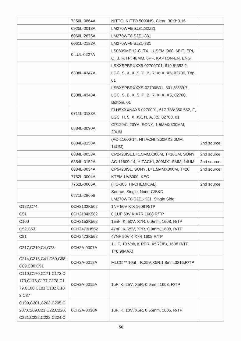
50
7250L-0864A NITTO, NITTO 5000NS, Clear, 30*3*0.16
6925L-0013A LM270WF6(SJZ1,S2Z2)
6060L-2675A LM270WF6-SJZ1-831
6061L-2182A LM270WF6-SJZ1-831
0ILUL-0227A LS0609MEH2-C1TX, LUSEM, 960, 6BIT, EPI,
C_B, R/TP, 48MM, 6PF, KAPTON-EN, ENG
6308L-4347A
LSXXSPBRXXX5-02700T01, 619.8*352.2,
LGC, S, X, X, S, P, B, R, X, X, X5, 02700, Top,
01
6308L-4348A
LSBXSPBRXXXS-02700B01, 601.3*339.7,
LGC, S, B, X, S, P, B, R, X, X, XS, 02700,
Bottom, 01
6711L-0133A FLH5XXXNAX5-0270001, 617.788*350.562, F,
LGC, H, 5, X, XX, N, A, X5, 02700, 01
6884L-0090A CP12941-20YA, SONY, 1.5MMX300MM,
20UM
6884L-0153A (AC-11600-14, HITACHI, 300MX2.0MM,
14UM) 2nd source
6884L-0053A CP2420ISL,L=1.5MMX300M, T=18UM, SONY 2nd source
6884L-0152A AC-11600-14, HITACHI, 300MX1.5MM, 14UM 2nd source
6884L-0034A CP5420ISL, SONY, L=1.5MMX300M, T=20 2nd source
7752L-0004A KTEM-UV3000, KEC
7752L-0005A (HC-305, HI-CHEMICAL) 2nd source
6871L-2865B Source, Single, None-C/SKD,
LM270WF6-SJZ1-K31, Single Side
C122,C74 0CH2102K562 1NF 50V K X 1608 R/TP
C51 0CH2104K562 0.1UF 50V K X7R 1608 R/TP
C100 0CH2153K562 15nF, K, 50V, X7R, 0.9mm, 1608, R/TP
C52,C53 0CH2473H562 47nF, K, 25V, X7R, 0.9mm, 1608, R/TP
C81 0CH2473K562 47NF 50V K X7R 1608 R/TP
C217,C219,C4,C73 0CH2A-0007A 1U F, 10 Volt, K PER, X5R(JB), 1608 R/TP,
T=0.9(MAX)
C214,C215,C41,C50,C88,
C89,C90,C91 0CH2A-0013A MLCC ** 10uf K,25V,X5R,1.8mm,3216,R/TP
C110,C170,C171,C172,C
173,C176,C177,C178,C1
79,C180,C181,C182,C18
3,C87
0CH2A-0015A 1uF, K, 25V, X5R, 0.9mm, 1608, R/TP
C199,C201,C203,C205,C
207,C209,C21,C22,C220,
C221,C222,C223,C224,C
0CH2A-0030A 1uF, K, 10V, X5R, 0.55mm, 1005, R/TP
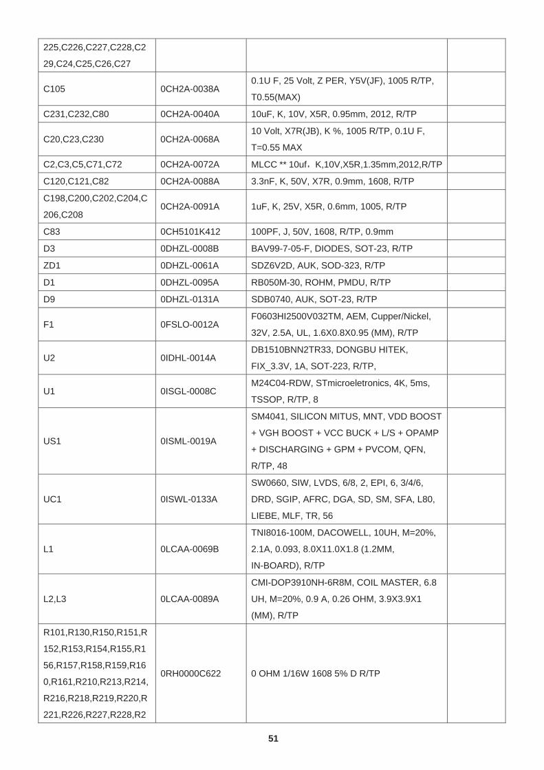
51
225,C226,C227,C228,C2
29,C24,C25,C26,C27
C105 0CH2A-0038A 0.1U F, 25 Volt, Z PER, Y5V(JF), 1005 R/TP,
T0.55(MAX)
C231,C232,C80 0CH2A-0040A 10uF, K, 10V, X5R, 0.95mm, 2012, R/TP
C20,C23,C230 0CH2A-0068A 10 Volt, X7R(JB), K %, 1005 R/TP, 0.1U F,
T=0.55 MAX
C2,C3,C5,C71,C72 0CH2A-0072A MLCC ** 10uf K,10V,X5R,1.35mm,2012,R/TP
C120,C121,C82 0CH2A-0088A 3.3nF, K, 50V, X7R, 0.9mm, 1608, R/TP
C198,C200,C202,C204,C
206,C208 0CH2A-0091A 1uF, K, 25V, X5R, 0.6mm, 1005, R/TP
C83 0CH5101K412 100PF, J, 50V, 1608, R/TP, 0.9mm
D3 0DHZL-0008B BAV99-7-05-F, DIODES, SOT-23, R/TP
ZD1 0DHZL-0061A SDZ6V2D, AUK, SOD-323, R/TP
D1 0DHZL-0095A RB050M-30, ROHM, PMDU, R/TP
D9 0DHZL-0131A SDB0740, AUK, SOT-23, R/TP
F1 0FSLO-0012A F0603HI2500V032TM, AEM, Cupper/Nickel,
32V, 2.5A, UL, 1.6X0.8X0.95 (MM), R/TP
U2 0IDHL-0014A DB1510BNN2TR33, DONGBU HITEK,
FIX_3.3V, 1A, SOT-223, R/TP,
U1 0ISGL-0008C M24C04-RDW, STmicroeletronics, 4K, 5ms,
TSSOP, R/TP, 8
US1 0ISML-0019A
SM4041, SILICON MITUS, MNT, VDD BOOST
+ VGH BOOST + VCC BUCK + L/S + OPAMP
+ DISCHARGING + GPM + PVCOM, QFN,
R/TP, 48
UC1 0ISWL-0133A
SW0660, SIW, LVDS, 6/8, 2, EPI, 6, 3/4/6,
DRD, SGIP, AFRC, DGA, SD, SM, SFA, L80,
LIEBE, MLF, TR, 56
L1 0LCAA-0069B
TNI8016-100M, DACOWELL, 10UH, M=20%,
2.1A, 0.093, 8.0X11.0X1.8 (1.2MM,
IN-BOARD), R/TP
L2,L3 0LCAA-0089A
CMI-DOP3910NH-6R8M, COIL MASTER, 6.8
UH, M=20%, 0.9 A, 0.26 OHM, 3.9X3.9X1
(MM), R/TP
R101,R130,R150,R151,R
152,R153,R154,R155,R1
56,R157,R158,R159,R16
0,R161,R210,R213,R214,
R216,R218,R219,R220,R
221,R226,R227,R228,R2
0RH0000C622 0 OHM 1/16W 1608 5% D R/TP
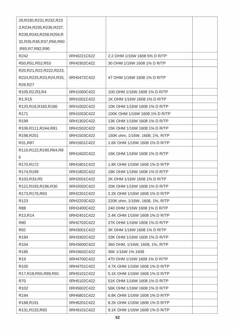
52
29,R230,R231,R232,R23
3,R234,R235,R236,R237,
R239,R243,R258,R259,R
32,R35,R36,R37,R56,R60
,R65,R7,R82,R90
R242 0RH0221C622 2.2 OHM 1/16W 1608 5% D R/TP
R50,R51,R52,R53 0RH0302C422 30 OHM 1/16W 1608 1% D R/TP
R20,R21,R22,R222,R223,
R224,R225,R23,R24,R25,
R26,R27
0RH0472C422 47 OHM 1/16W 1608 1% D R/TP
R105,R2,R3,R4 0RH1000C422 100 OHM 1/16W 1608 1% D R/TP
R1,R15 0RH1001C422 1K OHM 1/16W 1608 1% D R/TP
R120,R16,R183,R186 0RH1002C422 10K OHM 1/16W 1608 1% D R/TP
R171 0RH1003C422 100K OHM 1/16W 1608 1% D R/TP
R199 0RH1302C422 13K OHM 1/16W 1608 1% D R/TP
R106,R111,R244,R81 0RH1502C422 15K OHM 1/16W 1608 1% D R/TP
R198,R201 0RH1503C422 150K ohm, 1/16W, 1608, 1%, R/TP
R31,R87 0RH1601C422 1.6K OHM 1/16W 1608 1% D R/TP
R110,R122,R190,R64,R8
6 0RH1602C422 16K OHM 1/16W 1608 1% D R/TP
R170,R172 0RH1801C422 1.8K OHM 1/16W 1608 1% D R/TP
R174,R189 0RH1802C422 18K OHM 1/16W 1608 1% D R/TP
R103,R33,R5 0RH2001C422 2K OHM 1/16W 1608 1% D R/TP
R121,R193,R196,R30 0RH2002C422 20K OHM 1/16W 1608 1% D R/TP
R173,R176,R63 0RH2201C422 2.2K OHM 1/16W 1608 1% D R/TP
R123 0RH2203C422 220K ohm, 1/16W, 1608, 1%, R/TP
R88 0RH2400C422 240 OHM 1/16W 1608 1% D R/TP
R13,R14 0RH2401C422 2.4K OHM 1/16W 1608 1% D R/TP
R80 0RH2702C422 27K OHM 1/16W 1608 1% D R/TP
R92 0RH3001C422 3K OHM 1/16W 1608 1% D R/TP
R184 0RH3302C422 33K OHM 1/16W 1608 1% D R/TP
R104 0RH3600C422 360 OHM, 1/16W, 1608, 1%, R/TP
R185 0RH3602C422 36K 1/16W 1% 1608
R19 0RH4700C422 470 OHM 1/16W 1608 1% D R/TP
R100 0RH4701C422 4.7K OHM 1/16W 1608 1% D R/TP
R17,R18,R55,R89,R91 0RH5101C422 5.1K OHM 1/16W 1608 1% D R/TP
R70 0RH5102C422 51K OHM 1/16W 1608 1% D R/TP
R102 0RH5602C422 56K OHM 1/16W 1608 1% D R/TP
R194 0RH6801C422 6.8K OHM 1/16W 1608 1% D R/TP
R188,R191 0RH8201C422 8.2K OHM 1/16W 1608 1% D R/TP
R131,R133,R93 0RH9101C422 9.1K OHM 1/16W 1608 1% D R/TP
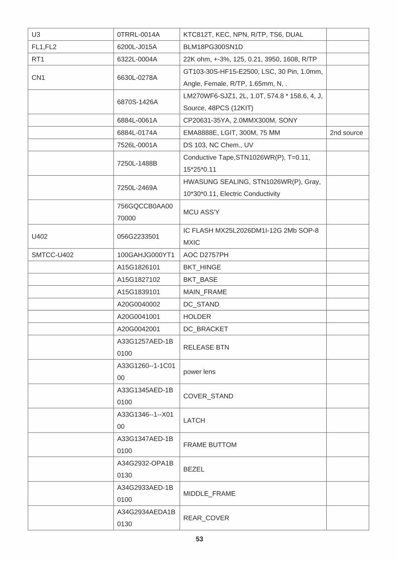
53
U3 0TRRL-0014A KTC812T, KEC, NPN, R/TP, TS6, DUAL
FL1,FL2 6200L-J015A BLM18PG300SN1D
RT1 6322L-0004A 22K ohm, +-3%, 125, 0.21, 3950, 1608, R/TP
CN1 6630L-0278A GT103-30S-HF15-E2500, LSC, 30 Pin, 1.0mm,
Angle, Female, R/TP, 1.65mm, N, .
6870S-1426A LM270WF6-SJZ1, 2L, 1.0T, 574.8 * 158.6, 4, J,
Source, 48PCS (12KIT)
6884L-0061A CP20631-35YA, 2.0MMX300M, SONY
6884L-0174A EMA8888E, LGIT, 300M, 75 M 2nd source
7526L-0001A DS 103, NC Chem., UV
7250L-1488B Conductive Tape,STN1026WR(P), T=0.11,
15*25*0.11
7250L-2469A HWASUNG SEALING, STN1026WR(P), Gray,
10*30*0.11, Electric Conductivity
756GQCCB0AA00
70000 MCU ASS'Y
U402 056G2233501 IC FLASH MX25L2026DM1I-12G 2Mb SOP-8
MXIC
SMTCC-U402 100GAHJG000YT1 AOC D2757PH
A15G1826101 BKT_HINGE
A15G1827102 BKT_BASE
A15G1839101 MAIN_FRAME
A20G0040002 DC_STAND
A20G0041001 HOLDER
A20G0042001 DC_BRACKET
A33G1257AED-1B
0100 RELEASE BTN
A33G1260--1-1C01
00 power lens
A33G1345AED-1B
0100 COVER_STAND
A33G1346--1--X01
00 LATCH
A33G1347AED-1B
0100 FRAME BUTTOM
A34G2932-OPA1B
0130 BEZEL
A34G2933AED-1B
0100 MIDDLE_FRAME
A34G2934AEDA1B
0130 REAR_COVER
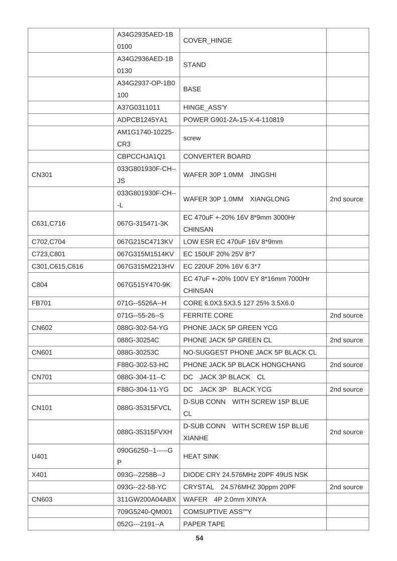
54
A34G2935AED-1B
0100 COVER_HINGE
A34G2936AED-1B
0130 STAND
A34G2937-OP-1B0
100 BASE
A37G0311011 HINGE_ASS'Y
ADPCB1245YA1 POWER G901-2A-15-X-4-110819
AM1G1740-10225-
CR3 screw
CBPCCHJA1Q1 CONVERTER BOARD
CN301 033G801930F-CH--
JS WAFER 30P 1.0MM JINGSHI
033G801930F-CH--
-L WAFER 30P 1.0MM XIANGLONG 2nd source
C631,C716 067G-315471-3K EC 470uF +-20% 16V 8*9mm 3000Hr
CHINSAN
C702,C704 067G215C4713KV LOW ESR EC 470uF 16V 8*9mm
C723,C801 067G315M1514KV EC 150UF 20% 25V 8*7
C301,C615,C616 067G315M2213HV EC 220UF 20% 16V 6.3*7
C804 067G515Y470-9K EC 47uF +-20% 100V EY 8*16mm 7000Hr
CHINSAN
FB701 071G--5526A--H CORE 6.0X3.5X3.5 127 25% 3.5X6.0
071G--55-26--S FERRITE CORE 2nd source
CN602 088G-302-54-YG PHONE JACK 5P GREEN YCG
088G-30254C PHONE JACK 5P GREEN CL 2nd source
CN601 088G-30253C NO-SUGGEST PHONE JACK 5P BLACK CL
F88G-302-53-HC PHONE JACK 5P BLACK HONGCHANG 2nd source
CN701 088G-304-11--C DC JACK 3P BLACK CL
F88G-304-11-YG DC JACK 3P BLACK YCG 2nd source
CN101 088G-35315FVCL D-SUB CONN WITH SCREW 15P BLUE
CL
088G-35315FVXH D-SUB CONN WITH SCREW 15P BLUE
XIANHE 2nd source
U401 090G6250--1-----G
P HEAT SINK
X401 093G--2258B--J DIODE CRY 24.576MHz 20PF 49US NSK
093G--22-58-YC CRYSTAL 24.576MHZ 30ppm 20PF 2nd source
CN603 311GW200A04ABX WAFER 4P 2.0mm XINYA
709G5240-QM001 COMSUPTIVE ASS""Y
052G---2191--A PAPER TAPE
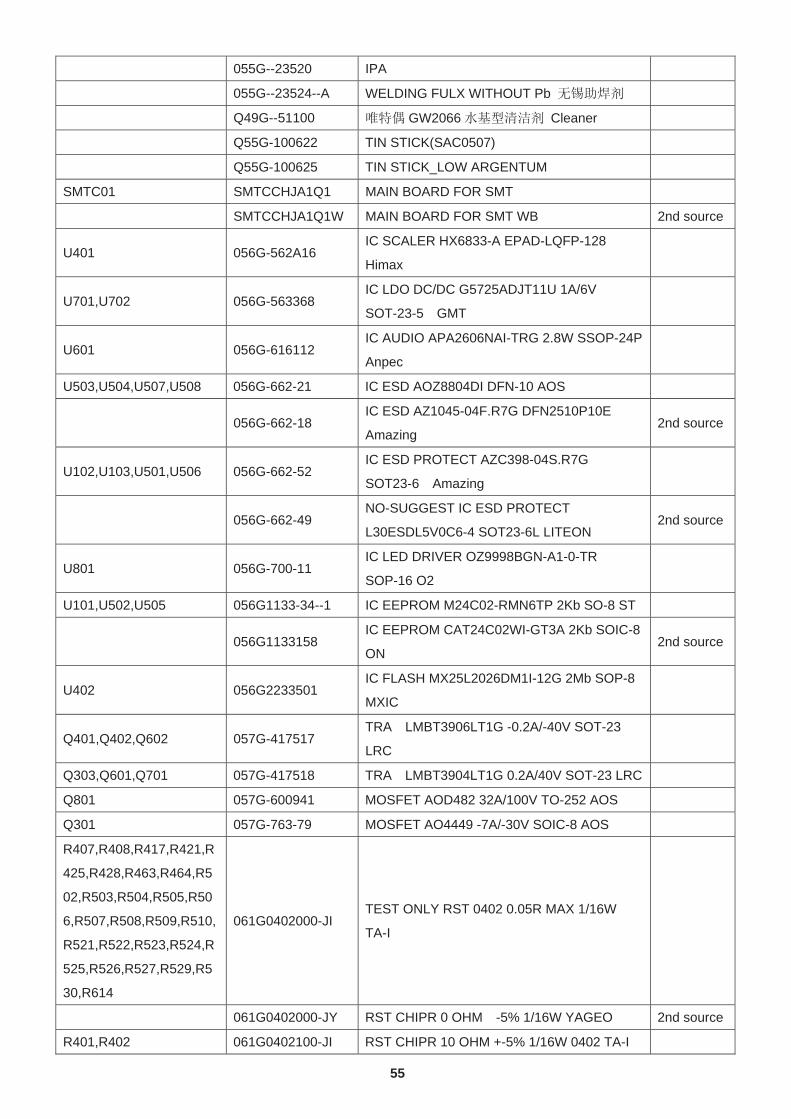
55
055G--23520 IPA
055G--23524--A WELDING FULX WITHOUT Pb
Q49G--51100 GW2066 Cleaner
Q55G-100622 TIN STICK(SAC0507)
Q55G-100625 TIN STICK_LOW ARGENTUM
SMTC01 SMTCCHJA1Q1 MAIN BOARD FOR SMT
SMTCCHJA1Q1W MAIN BOARD FOR SMT WB 2nd source
U401 056G-562A16 IC SCALER HX6833-A EPAD-LQFP-128
Himax
U701,U702 056G-563368 IC LDO DC/DC G5725ADJT11U 1A/6V
SOT-23-5 GMT
U601 056G-616112 IC AUDIO APA2606NAI-TRG 2.8W SSOP-24P
Anpec
U503,U504,U507,U508 056G-662-21 IC ESD AOZ8804DI DFN-10 AOS
056G-662-18 IC ESD AZ1045-04F.R7G DFN2510P10E
Amazing 2nd source
U102,U103,U501,U506 056G-662-52 IC ESD PROTECT AZC398-04S.R7G
SOT23-6 Amazing
056G-662-49 NO-SUGGEST IC ESD PROTECT
L30ESDL5V0C6-4 SOT23-6L LITEON 2nd source
U801 056G-700-11 IC LED DRIVER OZ9998BGN-A1-0-TR
SOP-16 O2
U101,U502,U505 056G1133-34--1 IC EEPROM M24C02-RMN6TP 2Kb SO-8 ST
056G1133158 IC EEPROM CAT24C02WI-GT3A 2Kb SOIC-8
ON 2nd source
U402 056G2233501 IC FLASH MX25L2026DM1I-12G 2Mb SOP-8
MXIC
Q401,Q402,Q602 057G-417517 TRA LMBT3906LT1G -0.2A/-40V SOT-23
LRC
Q303,Q601,Q701 057G-417518 TRA LMBT3904LT1G 0.2A/40V SOT-23 LRC
Q801 057G-600941 MOSFET AOD482 32A/100V TO-252 AOS
Q301 057G-763-79 MOSFET AO4449 -7A/-30V SOIC-8 AOS
R407,R408,R417,R421,R
425,R428,R463,R464,R5
02,R503,R504,R505,R50
6,R507,R508,R509,R510,
R521,R522,R523,R524,R
525,R526,R527,R529,R5
30,R614
061G0402000-JI TEST ONLY RST 0402 0.05R MAX 1/16W
TA-I
061G0402000-JY RST CHIPR 0 OHM -5% 1/16W YAGEO 2nd source
R401,R402 061G0402100-JI RST CHIPR 10 OHM +-5% 1/16W 0402 TA-I
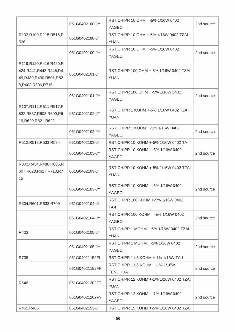
56
061G0402100-JY RST CHIPR 10 OHM -5% 1/16W 0402
YAGEO 2nd source
R103,R109,R115,R515,R
536 061G0402100-JT
RST CHIPR 10 OHM +-5% 1/16W 0402 TZAI
YUAN
061G0402100-JY RST CHIPR 10 OHM -5% 1/16W 0402
YAGEO 2nd source
R119,R120,R416,R420,R
424,R441,R443,R445,R4
49,R489,R490,R501,R52
8,R603,R606,R716
061G0402101-JT RST CHIPR 100 OHM +-5% 1/16W 0402 TZAI
YUAN
061G0402101-JY RST CHIPR 100 OHM -5% 1/16W 0402
YAGEO 2nd source
R107,R112,R511,R517,R
532,R537,R608,R609,R6
19,R620,R621,R622
061G0402102-JT RST CHIPR 1 KOHM +-5% 1/16W 0402 TZAI
YUAN
061G0402102-JY RST CHIPR 1 KOHM -5% 1/16W 0402
YAGEO 2nd source
R512,R513,R533,R534 061G0402103-JI RST CHIPR 10 KOHM +-5% 1/16W 0402 TA-I
061G0402103-JY RST CHIPR 10 KOHM -5% 1/16W 0402
YAGEO 2nd source
R303,R454,R480,R605,R
607,R623,R627,R713,R7
15
061G0402103-JT RST CHIPR 10 KOHM +-5% 1/16W 0402 TZAI
YUAN
061G0402103-JY RST CHIPR 10 KOHM -5% 1/16W 0402
YAGEO 2nd source
R304,R601,R633,R709 061G0402104-JI RST CHIPR 100 KOHM +-5% 1/16W 0402
TA-I
061G0402104-JY RST CHIPR 100 KOHM -5% 1/16W 0402
YAGEO 2nd source
R403 061G0402105-JT RST CHIPR 1 MOHM +-5% 1/16W 0402 TZAI
YUAN
061G0402105-JY RST CHIPR 1 MOHM -5% 1/16W 0402
YAGEO 2nd source
R705 061G04021152FI RST CHIPR 11.5 KOHM +-1% 1/16W TA-I
061G04021152FF RST CHIPR 11.5 KOHM -1% 1/16W
FENGHUA 2nd source
R646 061G04021202FT RST CHIPR 12 KOHM +-1% 1/16W 0402 TZAI
YUAN
061G04021202FY RST CHIPR 12 KOHM -1% 1/16W 0402
YAGEO 2nd source
R465,R466 061G0402153-JT RST CHIPR 15 KOHM +-5% 1/16W 0402 TZAI
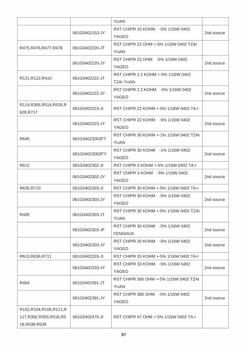
57
YUAN
061G0402153-JY RST CHIPR 15 KOHM -5% 1/16W 0402
YAGEO 2nd source
R475,R476,R477,R478 061G0402220-JT RST CHIPR 22 OHM +-5% 1/16W 0402 TZAI
YUAN
061G0402220-JY RST CHIPR 22 OHM -5% 1/16W 0402
YAGEO 2nd source
R121,R122,R410 061G0402222-JT RST CHIPR 2.2 KOHM +-5% 1/16W 0402
TZAI YUAN
061G0402222-JY RST CHIPR 2.2 KOHM -5% 1/16W 0402
YAGEO 2nd source
R114,R306,R514,R535,R
628,R717 061G0402223-JI RST CHIPR 22 KOHM +-5% 1/16W 0402 TA-I
061G0402223-JY RST CHIPR 22 KOHM -5% 1/16W 0402
YAGEO 2nd source
R645 061G04023002FT RST CHIPR 30 KOHM +-1% 1/16W 0402 TZAI
YUAN
061G04023002FY RST CHIPR 30 KOHM -1% 1/16W 0402
YAGEO 2nd source
R612 061G0402302-JI RST CHIPR 3 KOHM +-5% 1/16W 0402 TA-I
061G0402302-JY RST CHIPR 3 KOHM -5% 1/16W 0402
YAGEO 2nd source
R635,R710 061G0402303-JI RST CHIPR 30 KOHM +-5% 1/16W 0402 TA-I
061G0402303-JY RST CHIPR 30 KOHM -5% 1/16W 0402
YAGEO 2nd source
R405 061G0402303-JT RST CHIPR 30 KOHM +-5% 1/16W 0402 TZAI
YUAN
061G0402303-JF RST CHIPR 30 KOHM -5% 1/16W 0402
FENGHUA 2nd source
061G0402303-JY RST CHIPR 30 KOHM -5% 1/16W 0402
YAGEO 2nd source
R613,R636,R711 061G0402333-JI RST CHIPR 33 KOHM +-5% 1/16W 0402 TA-I
061G0402333-JY RST CHIPR 33 KOHM -5% 1/16W 0402
YAGEO 2nd source
R404 061G0402391-JT RST CHIPR 390 OHM +-5% 1/16W 0402 TZAI
YUAN
061G0402391-JY RST CHIPR 390 OHM -5% 1/16W 0402
YAGEO 2nd source
R102,R104,R106,R111,R
117,R392,R393,R516,R5
18,R538,R539
061G0402470-JI RST CHIPR 47 OHM +-5% 1/16W 0402 TA-I
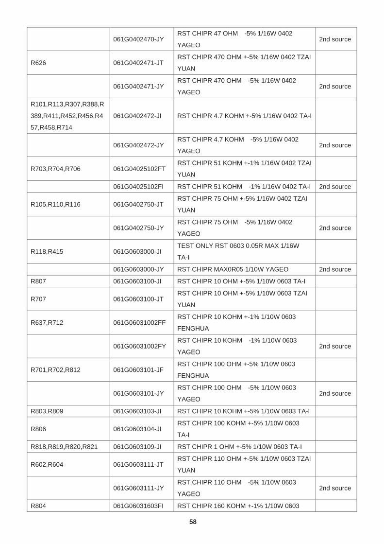
58
061G0402470-JY RST CHIPR 47 OHM -5% 1/16W 0402
YAGEO 2nd source
R626 061G0402471-JT RST CHIPR 470 OHM +-5% 1/16W 0402 TZAI
YUAN
061G0402471-JY RST CHIPR 470 OHM -5% 1/16W 0402
YAGEO 2nd source
R101,R113,R307,R388,R
389,R411,R452,R456,R4
57,R458,R714
061G0402472-JI RST CHIPR 4.7 KOHM +-5% 1/16W 0402 TA-I
061G0402472-JY RST CHIPR 4.7 KOHM -5% 1/16W 0402
YAGEO 2nd source
R703,R704,R706 061G04025102FT RST CHIPR 51 KOHM +-1% 1/16W 0402 TZAI
YUAN
061G04025102FI RST CHIPR 51 KOHM -1% 1/16W 0402 TA-I 2nd source
R105,R110,R116 061G0402750-JT RST CHIPR 75 OHM +-5% 1/16W 0402 TZAI
YUAN
061G0402750-JY RST CHIPR 75 OHM -5% 1/16W 0402
YAGEO 2nd source
R118,R415 061G0603000-JI TEST ONLY RST 0603 0.05R MAX 1/16W
TA-I
061G0603000-JY RST CHIPR MAX0R05 1/10W YAGEO 2nd source
R807 061G0603100-JI RST CHIPR 10 OHM +-5% 1/10W 0603 TA-I
R707 061G0603100-JT RST CHIPR 10 OHM +-5% 1/10W 0603 TZAI
YUAN
R637,R712 061G06031002FF RST CHIPR 10 KOHM +-1% 1/10W 0603
FENGHUA
061G06031002FY RST CHIPR 10 KOHM -1% 1/10W 0603
YAGEO 2nd source
R701,R702,R812 061G0603101-JF RST CHIPR 100 OHM +-5% 1/10W 0603
FENGHUA
061G0603101-JY RST CHIPR 100 OHM -5% 1/10W 0603
YAGEO 2nd source
R803,R809 061G0603103-JI RST CHIPR 10 KOHM +-5% 1/10W 0603 TA-I
R806 061G0603104-JI RST CHIPR 100 KOHM +-5% 1/10W 0603
TA-I
R818,R819,R820,R821 061G0603109-JI RST CHIPR 1 OHM +-5% 1/10W 0603 TA-I
R602,R604 061G0603111-JT RST CHIPR 110 OHM +-5% 1/10W 0603 TZAI
YUAN
061G0603111-JY RST CHIPR 110 OHM -5% 1/10W 0603
YAGEO 2nd source
R804 061G06031603FI RST CHIPR 160 KOHM +-1% 1/10W 0603
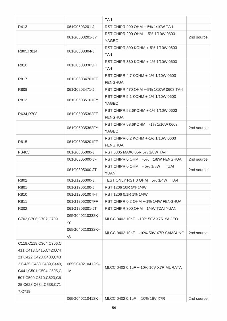
59
TA-I
R413 061G0603201-JI RST CHIPR 200 OHM +-5% 1/10W TA-I
061G0603201-JY RST CHIPR 200 OHM -5% 1/10W 0603
YAGEO 2nd source
R805,R814 061G0603304-JI RST CHIPR 300 KOHM +-5% 1/10W 0603
TA-I
R816 061G06033303FI RST CHIPR 330 KOHM +-1% 1/10W 0603
TA-I
R817 061G06034701FF RST CHIPR 4.7 KOHM +-1% 1/10W 0603
FENGHUA
R808 061G0603471-JI RST CHIPR 470 OHM +-5% 1/10W 0603 TA-I
R813 061G06035101FY RST CHIPR 5.1 KOHM +-1% 1/10W 0603
YAGEO
R634,R708 061G06035362FF RST CHIPR 53.6KOHM +-1% 1/10W 0603
FENGHUA
061G06035362FY RST CHIPR 53.6KOHM -1% 1/10W 0603
YAGEO 2nd source
R815 061G06036201FF RST CHIPR 6.2 KOHM +-1% 1/10W 0603
FENGHUA
FB405 061G0805000-JI RST 0805 MAX0.05R 5% 1/8W TA-I
061G0805000-JF RST CHIPR 0 OHM -5% 1/8W FENGHUA 2nd source
061G0805000-JT RST CHIPR 0 OHM - 5% 1/8W TZAI
YUAN 2nd source
R802 061G1206000-JI TEST ONLY RST 0 OHM 5% 1/4W TA-I
R801 061G1206100-JI RST 1206 10R 5% 1/4W
R810 061G12061007FT RST 1206 0.1R 1% 1/4W
R811 061G12062007FF RST CHIPR 0.2 OHM +-1% 1/4W FENGHUA
R302 061G1206301-JT RST CHIPR 300 OHM 1/4W TZAI YUAN
C703,C706,C707,C709 065G040210332K--
-Y MLCC 0402 10nF +-10% 50V X7R YAGEO
065G040210332K--
-A MLCC 0402 10nF -10% 50V X7R SAMSUNG 2nd source
C118,C119,C304,C306,C
411,C413,C415,C420,C4
21,C422,C423,C430,C43
2,C435,C438,C439,C440,
C441,C501,C504,C505,C
507,C509,C510,C623,C6
25,C628,C634,C638,C71
7,C719
065G040210412K--
-M MLCC 0402 0.1uF +-10% 16V X7R MURATA
065G040210412K-- MLCC 0402 0.1uF -10% 16V X7R 2nd source
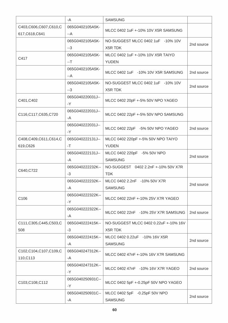
60
-A SAMSUNG
C403,C606,C607,C610,C
617,C618,C641
065G0402105A5K-
--A MLCC 0402 1uF +-10% 10V X5R SAMSUNG
065G0402105A5K-
--3
NO-SUGGEST MLCC 0402 1uF -10% 10V
X5R TDK 2nd source
C417 065G0402105A5K-
--T
MLCC 0402 1uF +-10% 10V X5R TAIYO
YUDEN
065G0402105A5K-
--A MLCC 0402 1uF -10% 10V X5R SAMSUNG 2nd source
065G0402105A5K-
--3
NO-SUGGEST MLCC 0402 1uF -10% 10V
X5R TDK 2nd source
C401,C402 065G040220031J--
-Y MLCC 0402 20pF +-5% 50V NPO YAGEO
C116,C117,C635,C720 065G040222031J--
-A MLCC 0402 22pF +-5% 50V NPO SAMSUNG
065G040222031J--
-Y MLCC 0402 22pF -5% 50V NPO YAGEO 2nd source
C408,C409,C611,C614,C
619,C626
065G040222131J--
-T
MLCC 0402 220pF +-5% 50V NPO TAIYO
YUDEN
065G040222131J--
-A
MLCC 0402 220pF -5% 50V NPO
SAMSUNG 2nd source
C640,C722 065G040222232K--
-3
NO-SUGGEST 0402 2.2nF +-10% 50V X7R
TDK
065G040222232K--
-A
MLCC 0402 2.2nF -10% 50V X7R
SAMSUNG 2nd source
C106 065G040222322K--
-Y MLCC 0402 22nF +-10% 25V X7R YAGEO
065G040222322K--
-A MLCC 0402 22nF -10% 25V X7R SAMSUNG 2nd source
C111,C305,C445,C503,C
508
065G040222415K--
-3
NO-SUGGEST MLCC 0402 0.22uF +-10% 16V
X5R TDK
065G040222415K--
-A
MLCC 0402 0.22uF -10% 16V X5R
SAMSUNG 2nd source
C102,C104,C107,C109,C
110,C113
065G040247312K--
-A MLCC 0402 47nF +-10% 16V X7R SAMSUNG
065G040247312K--
-Y MLCC 0402 47nF -10% 16V X7R YAGEO 2nd source
C103,C108,C112 065G040250931C--
-Y MLCC 0402 5pF +-0.25pF 50V NPO YAGEO
065G040250931C--
-A
MLCC 0402 5pF -0.25pF 50V NPO
SAMSUNG 2nd source
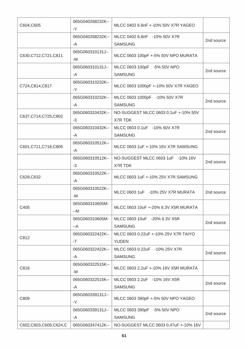
61
C604,C605 065G040268232K--
-Y MLCC 0402 6.8nF +-10% 50V X7R YAGEO
065G040268232K--
-A
MLCC 0402 6.8nF -10% 50V X7R
SAMSUNG 2nd source
C630,C712,C721,C811 065G060310131J--
-M MLCC 0603 100pF +-5% 50V NPO MURATA
065G060310131J--
-A
MLCC 0603 100pF -5% 50V NPO
SAMSUNG 2nd source
C724,C814,C817 065G060310232K--
-Y MLCC 0603 1000pF +-10% 50V X7R YAGEO
065G060310232K--
-A
MLCC 0603 1000pF -10% 50V X7R
SAMSUNG 2nd source
C637,C714,C725,C802 065G060310432K--
-3
NO-SUGGEST MLCC 0603 0.1uF +-10% 50V
X7R TDK
065G060310432K--
-A
MLCC 0603 0.1uF -10% 50V X7R
SAMSUNG 2nd source
C601,C711,C718,C805 065G060310512K--
-A MLCC 0603 1uF +-10% 16V X7R SAMSUNG
065G060310512K--
-3
NO-SUGGEST MLCC 0603 1uF -10% 16V
X7R TDK 2nd source
C629,C632 065G060310522K--
-A MLCC 0603 1uF +-10% 25V X7R SAMSUNG
065G060310522K--
-M MLCC 0603 1uF -10% 25V X7R MURATA 2nd source
C405 065G060310605M-
--M MLCC 0603 10uF +-20% 6.3V X5R MURATA
065G060310605M-
--A
MLCC 0603 10uF -20% 6.3V X5R
SAMSUNG 2nd source
C812 065G060322422K--
-T
MLCC 0603 0.22uF +-10% 25V X7R TAIYO
YUDEN
065G060322422K--
-A
MLCC 0603 0.22uF -10% 25V X7R
SAMSUNG 2nd source
C816 065G060322515K--
-M MLCC 0603 2.2uF +-10% 16V X5R MURATA
065G060322515K--
-A
MLCC 0603 2.2uF -10% 16V X5R
SAMSUNG 2nd source
C809 065G060339131J--
-Y MLCC 0603 390pF +-5% 50V NPO YAGEO
065G060339131J--
-A
MLCC 0603 390pF -5% 50V NPO
SAMSUNG 2nd source
C602,C603,C609,C624,C 065G060347412K-- NO-SUGGEST MLCC 0603 0.47uF +-10% 16V
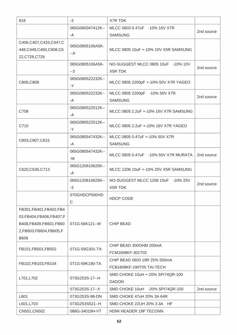
62
818 -3 X7R TDK
065G060347412K--
-A
MLCC 0603 0.47uF -10% 16V X7R
SAMSUNG 2nd source
C406,C407,C433,C447,C
448,C449,C450,C608,C6
22,C728,C729
065G0805106A5K-
--A MLCC 0805 10uF +-10% 10V X5R SAMSUNG
065G0805106A5K-
--3
NO-SUGGEST MLCC 0805 10uF -10% 10V
X5R TDK 2nd source
C806,C808 065G080522232K--
-Y MLCC 0805 2200pF +-10% 50V X7R YAGEO
065G080522232K--
-A
MLCC 0805 2200pF -10% 50V X7R
SAMSUNG 2nd source
C708 065G080522512K--
-A MLCC 0805 2.2uF +-10% 16V X7R SAMSUNG
C710 065G080522512K--
-Y MLCC 0805 2.2uF +-10% 16V X7R YAGEO
C803,C807,C815 065G080547432K--
-A
MLCC 0805 0.47uF +-10% 50V X7R
SAMSUNG
065G080547432K--
-M MLCC 0805 0.47uF -10% 50V X7R MURATA 2nd source
C620,C636,C713 065G120610625K--
-A MLCC 1206 10uF +-10% 25V X5R SAMSUNG
065G120610625K--
-3
NO-SUGGEST MLCC 1206 10uF -10% 25V
X5R TDK 2nd source
070GHDCP500HD
C HDCP CODE
FB301,FB401,FB402,FB4
03,FB404,FB406,FB407,F
B408,FB409,FB601,FB60
2,FB603,FB604,FB605,F
B606
071G-56K121--M CHIP BEAD
FB101,FB501,FB502 071G-59G301-TA CHIP BEAD 300OHM 200mA
FCM1608KF-301T02
FB102,FB103,FB104 071G-59K190-TA CHIP BEAD 0603 19R 25% 500mA
FCB1608KF-190T05 TAI-TECH
L701,L702 073G253S-17--H SMD CHOKE 10uH +-20% SPI74QR-100
DADON
073G253S-17--X SMD CHOKE 10uH -20% SPI74QR-100 2nd source
L801 073G253S-98-DN SMD CHOKE 47uH 20% 3A 64R
L601,L703 073G253S521--H SMD CHOKE 22UH 20% 3.3A HF
CN501,CN502 088G-34019H-VT HDMI HEADER 19P TECONN
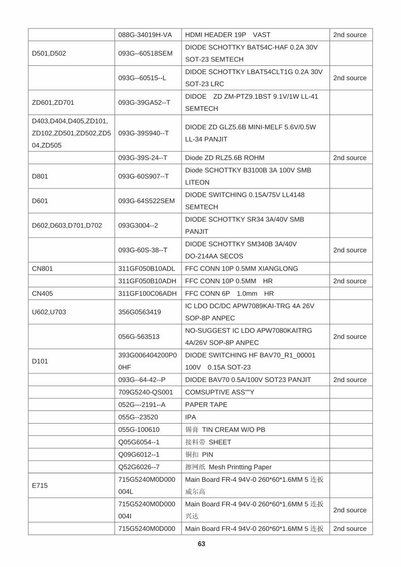
63
088G-34019H-VA HDMI HEADER 19P VAST 2nd source
D501,D502 093G--60518SEM DIODE SCHOTTKY BAT54C-HAF 0.2A 30V
SOT-23 SEMTECH
093G--60515--L DIDOE SCHOTTKY LBAT54CLT1G 0.2A 30V
SOT-23 LRC 2nd source
ZD601,ZD701 093G-39GA52--T DIDOE ZD ZM-PTZ9.1BST 9.1V/1W LL-41
SEMTECH
D403,D404,D405,ZD101,
ZD102,ZD501,ZD502,ZD5
04,ZD505
093G-39S940--T DIODE ZD GLZ5.6B MINI-MELF 5.6V/0.5W
LL-34 PANJIT
093G-39S-24--T Diode ZD RLZ5.6B ROHM 2nd source
D801 093G-60S907--T Diode SCHOTTKY B3100B 3A 100V SMB
LITEON
D601 093G-64S522SEM DIODE SWITCHING 0.15A/75V LL4148
SEMTECH
D602,D603,D701,D702 093G3004--2 DIODE SCHOTTKY SR34 3A/40V SMB
PANJIT
093G-60S-38--T DIODE SCHOTTKY SM340B 3A/40V
DO-214AA SECOS 2nd source
CN801 311GF050B10ADL FFC CONN 10P 0.5MM XIANGLONG
311GF050B10ADH FFC CONN 10P 0.5MM HR 2nd source
CN405 311GF100C06ADH FFC CONN 6P 1.0mm HR
U602,U703 356G0563419 IC LDO DC/DC APW7089KAI-TRG 4A 26V
SOP-8P ANPEC
056G-563513 NO-SUGGEST IC LDO APW7080KAITRG
4A/26V SOP-8P ANPEC 2nd source
D101 393G006404200P0
0HF
DIODE SWITCHING HF BAV70_R1_00001
100V 0.15A SOT-23
093G--64-42--P DIODE BAV70 0.5A/100V SOT23 PANJIT 2nd source
709G5240-QS001 COMSUPTIVE ASS""Y
052G---2191--A PAPER TAPE
055G--23520 IPA
055G-100610 TIN CREAM W/O PB
Q05G6054--1 SHEET
Q09G6012--1 PIN
Q52G6026--7 Mesh Printting Paper
E715 715G5240M0D000
004L
Main Board FR-4 94V-0 260*60*1.6MM 5
715G5240M0D000
004I
Main Board FR-4 94V-0 260*60*1.6MM 5
2nd source
715G5240M0D000 Main Board FR-4 94V-0 260*60*1.6MM 5 2nd source
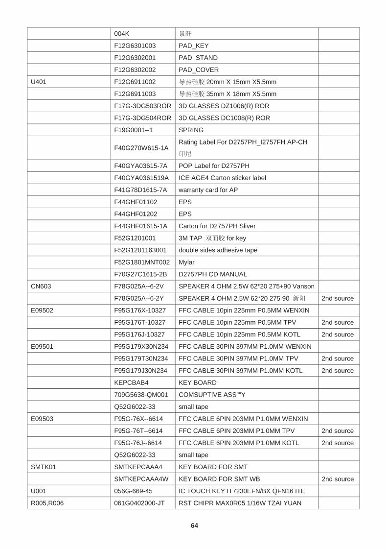
64
004K
F12G6301003 PAD_KEY
F12G6302001 PAD_STAND
F12G6302002 PAD_COVER
U401 F12G6911002 20mm X 15mm X5.5mm
F12G6911003 35mm X 18mm X5.5mm
F17G-3DG503ROR 3D GLASSES DZ1006(R) ROR
F17G-3DG504ROR 3D GLASSES DC1008(R) ROR
F19G0001--1 SPRING
F40G270W615-1A Rating Label For D2757PH_I2757FH AP-CH
F40GYA03615-7A POP Label for D2757PH
F40GYA0361519A ICE AGE4 Carton sticker label
F41G78D1615-7A warranty card for AP
F44GHF01102 EPS
F44GHF01202 EPS
F44GHF01615-1A Carton for D2757PH Sliver
F52G1201001 3M TAP for key
F52G1201163001 double sides adhesive tape
F52G1801MNT002 Mylar
F70G27C1615-2B D2757PH CD MANUAL
CN603 F78G025A--6-2V SPEAKER 4 OHM 2.5W 62*20 275+90 Vanson
F78G025A--6-2Y SPEAKER 4 OHM 2.5W 62*20 275 90 2nd source
E09502 F95G176X-10327 FFC CABLE 10pin 225mm P0.5MM WENXIN
F95G176T-10327 FFC CABLE 10pin 225mm P0.5MM TPV 2nd source
F95G176J-10327 FFC CABLE 10pin 225mm P0.5MM KOTL 2nd source
E09501 F95G179X30N234 FFC CABLE 30PIN 397MM P1.0MM WENXIN
F95G179T30N234 FFC CABLE 30PIN 397MM P1.0MM TPV 2nd source
F95G179J30N234 FFC CABLE 30PIN 397MM P1.0MM KOTL 2nd source
KEPCBAB4 KEY BOARD
709G5638-QM001 COMSUPTIVE ASS""Y
Q52G6022-33 small tape
E09503 F95G-76X--6614 FFC CABLE 6PIN 203MM P1.0MM WENXIN
F95G-76T--6614 FFC CABLE 6PIN 203MM P1.0MM TPV 2nd source
F95G-76J--6614 FFC CABLE 6PIN 203MM P1.0MM KOTL 2nd source
Q52G6022-33 small tape
SMTK01 SMTKEPCAAA4 KEY BOARD FOR SMT
SMTKEPCAAA4W KEY BOARD FOR SMT WB 2nd source
U001 056G-669-45 IC TOUCH KEY IT7230EFN/BX QFN16 ITE
R005,R006 061G0402000-JT RST CHIPR MAX0R05 1/16W TZAI YUAN
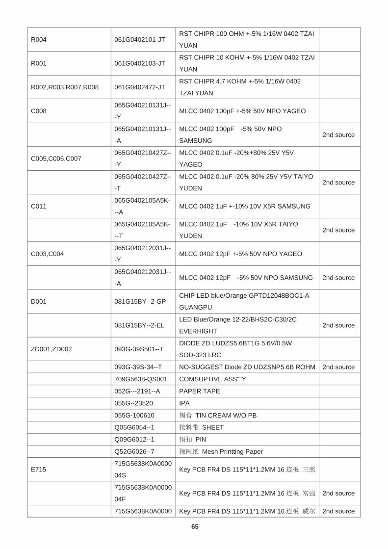
65
R004 061G0402101-JT RST CHIPR 100 OHM +-5% 1/16W 0402 TZAI
YUAN
R001 061G0402103-JT RST CHIPR 10 KOHM +-5% 1/16W 0402 TZAI
YUAN
R002,R003,R007,R008 061G0402472-JT RST CHIPR 4.7 KOHM +-5% 1/16W 0402
TZAI YUAN
C008 065G040210131J--
-Y MLCC 0402 100pF +-5% 50V NPO YAGEO
065G040210131J--
-A
MLCC 0402 100pF -5% 50V NPO
SAMSUNG 2nd source
C005,C006,C007 065G040210427Z--
-Y
MLCC 0402 0.1uF -20%+80% 25V Y5V
YAGEO
065G040210427Z--
-T
MLCC 0402 0.1uF -20% 80% 25V Y5V TAIYO
YUDEN 2nd source
C011 065G0402105A5K-
--A MLCC 0402 1uF +-10% 10V X5R SAMSUNG
065G0402105A5K-
--T
MLCC 0402 1uF -10% 10V X5R TAIYO
YUDEN 2nd source
C003,C004 065G040212031J--
-Y MLCC 0402 12pF +-5% 50V NPO YAGEO
065G040212031J--
-A MLCC 0402 12pF -5% 50V NPO SAMSUNG 2nd source
D001 081G15BY--2-GP CHIP LED blue/Orange GPTD12048BOC1-A
GUANGPU
081G15BY--2-EL LED Blue/Orange 12-22/BHS2C-C30/2C
EVERHIGHT 2nd source
ZD001,ZD002 093G-39S501--T DIODE ZD LUDZS5.6BT1G 5.6V/0.5W
SOD-323 LRC
093G-39S-34--T NO-SUGGEST Diode ZD UDZSNP5.6B ROHM 2nd source
709G5638-QS001 COMSUPTIVE ASS""Y
052G---2191--A PAPER TAPE
055G--23520 IPA
055G-100610 TIN CREAM W/O PB
Q05G6054--1 SHEET
Q09G6012--1 PIN
Q52G6026--7 Mesh Printting Paper
E715 715G5638K0A0000
04S Key PCB FR4 DS 115*11*1.2MM 16
715G5638K0A0000
04F Key PCB FR4 DS 115*11*1.2MM 16 2nd source
715G5638K0A0000 Key PCB FR4 DS 115*11*1.2MM 16 2nd source
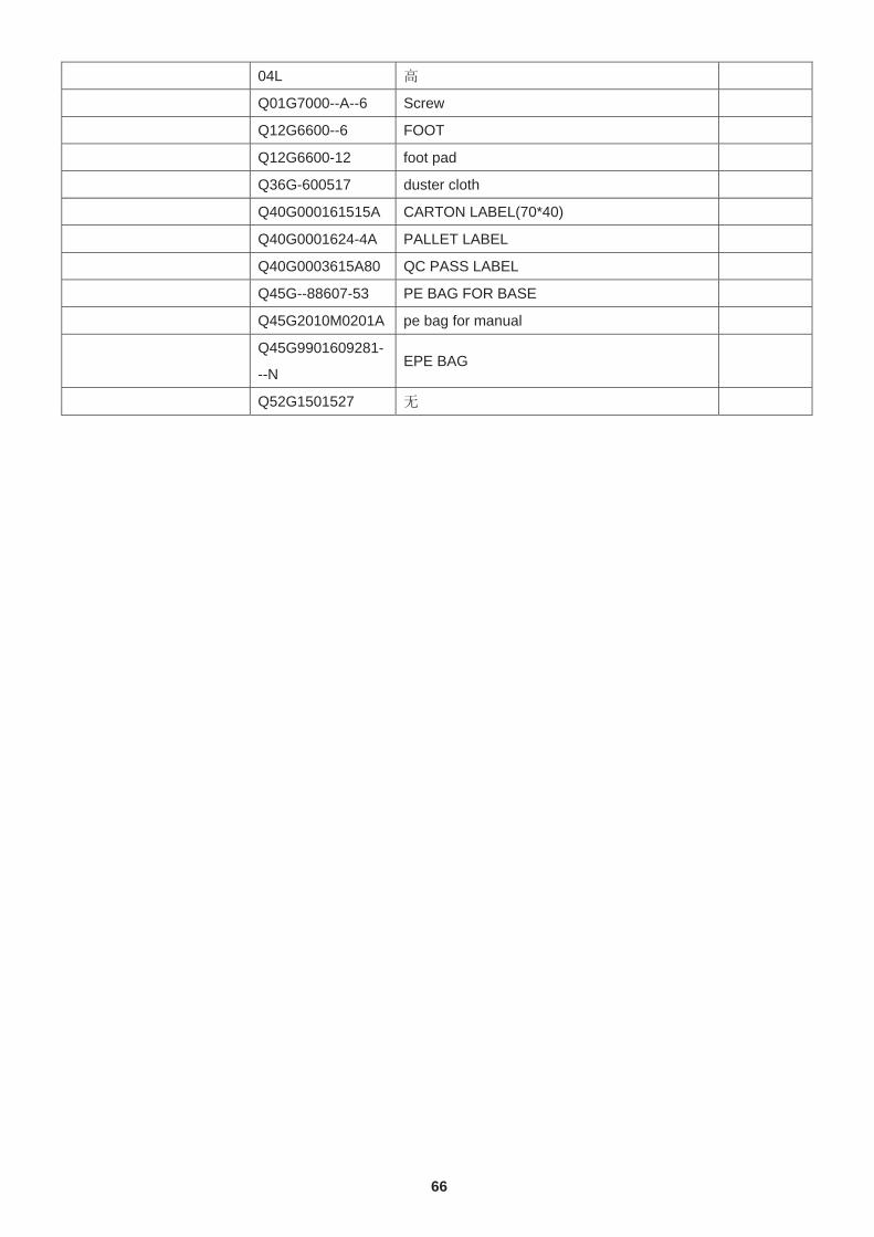
66
04L
Q01G7000--A--6 Screw
Q12G6600--6 FOOT
Q12G6600-12 foot pad
Q36G-600517 duster cloth
Q40G000161515A CARTON LABEL(70*40)
Q40G0001624-4A PALLET LABEL
Q40G0003615A80 QC PASS LABEL
Q45G--88607-53 PE BAG FOR BASE
Q45G2010M0201A pe bag for manual
Q45G9901609281-
--N EPE BAG
Q52G1501527