contentscms3.koreatech.ac.kr/sites/yjjang/down/emsoc/mod05a_arm... · 2016-10-31 · uart flash...
TRANSCRIPT
4Module13 ARM기반 SoC Design(I)
ContentsContents
Excalibur Devices 의 구조와 기능STRIPE을 구성하는 방법Bus Function Simulation의 개념 이해실습
설계변경후 실습
5Module13 ARM기반 SoC Design(I)
Excalibur DevicesExcalibur Devices
Industry-standard ARM922T™ 32-bit RISC processor core operating at up to 200 MHz
ARMv4T instruction set with Thumb® extensionsMemory management unit (MMU) included for real-time operating system (RTOS) supportHarvard cache architecture with 64-way set associative separate 8-Kbyte instruction and 8-Kbyte data caches
APEX™ 20KE-like programmable logic architecture ranging from 100,000 to 1,000,000 gatesAdvanced bus architecture based on advanced microcontroller bus architecture (AMBA™) high-performance bus (AHB)Embedded programmable on-chip peripherals
ETM9™ embedded trace module to assist software debuggingFlexible interrupt controllerUniversal asynchronous receiver/transmitter (UART)General-purpose timerWatchdog timer
1.8-V supply voltage, but many I/O standards supported
6Module13 ARM기반 SoC Design(I)
Excalibur Devices featuresExcalibur Devices features
Advanced memory supportInternal single-port SRAM up to 256 KbytesInternal dual-port SRAM up to 128 KbytesInternal SDRAM controller
Single data-rate (SDR) and double data-rate (DDR) support Up to 512 MbytesData rates to 133 (266) MHz
Expansion bus interface (EBI)Compatible with industry-standard flash memory, SRAMs, and peripheral devicesFour devices, each up to 32 Mbytes
Multiple and separate clock domains controlled by software programmable phased-lock loops(PLLs) for embedded processor, SDRAM, and PLD
7Module13 ARM기반 SoC Design(I)
Software Development EnvironmentSoftware Development Environment
PLD configuration/reconfiguration possible via the embedded processor softwareExtended Quartus® II development environment for Excalibur support
Integrated hardware and software development environmentMegaWizard® Plug-In interface configures the embedded processor, PLD, bus connections, and peripheralsC/C++ compiler, source-level debugger, and RTOS support
Fully configurable memory mapExtensive embedded system debug facilities
SignalTap® embedded logic analyzerARM® JTAG processor debug supportReal-time data/instruction processor traceBackground debug monitoring via the IEEE Std. 1149.1 (JTAG) interface
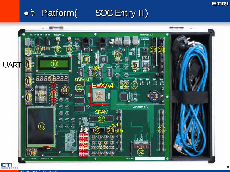
8Module13 ARM기반 SoC Design(I)
사용 Platform(한백 SOC Entry II)사용 Platform(한백 SOC Entry II)
EPXA4
SRAM
SDRAM
FLASHUART
Byte blaster
9Module13 ARM기반 SoC Design(I)
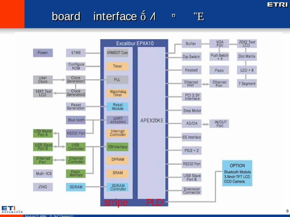
한백 board의 interface 되어 있는 회로한백 board의 interface 되어 있는 회로
stripe PLD
10Module13 ARM기반 SoC Design(I)
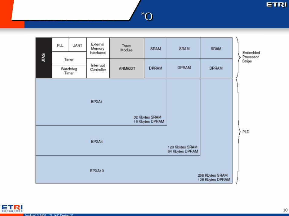
Excalibur Devices 의 종류Excalibur Devices 의 종류
11Module13 ARM기반 SoC Design(I)
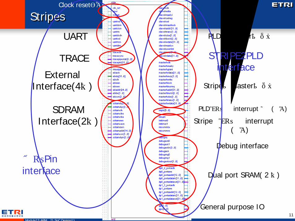
StripesStripes
UART
External Interface(4개)
SDRAM Interface(2개)
PLD가 master가 될때
Stripe가 master가 될때
PLD로부터의 interrupt 신호(입력)
TRACE
Stripe으로부터의 interrupt 신호(출력)
외부 Pin interface
Debug interface
Dual port SRAM( 2 개)
General purpose IO
STRIPE2PLD interface
Clock reset관련
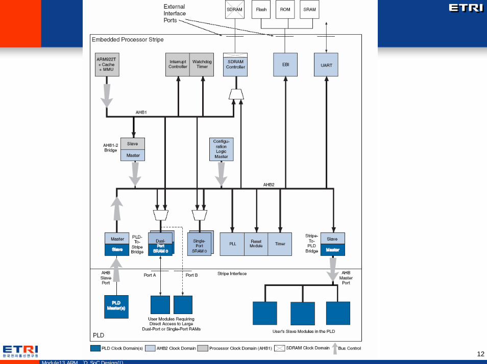
12Module13 ARM기반 SoC Design(I)
13Module13 ARM기반 SoC Design(I)
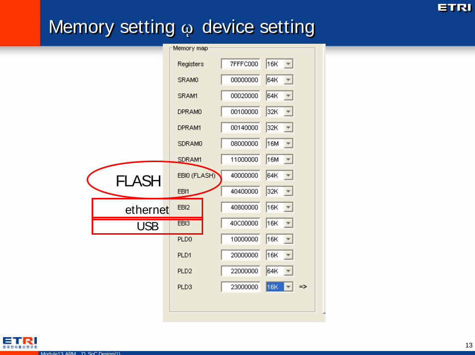
Memory setting 및 device settingMemory setting 및 device setting
ethernetUSB
FLASH
14Module13 ARM기반 SoC Design(I)
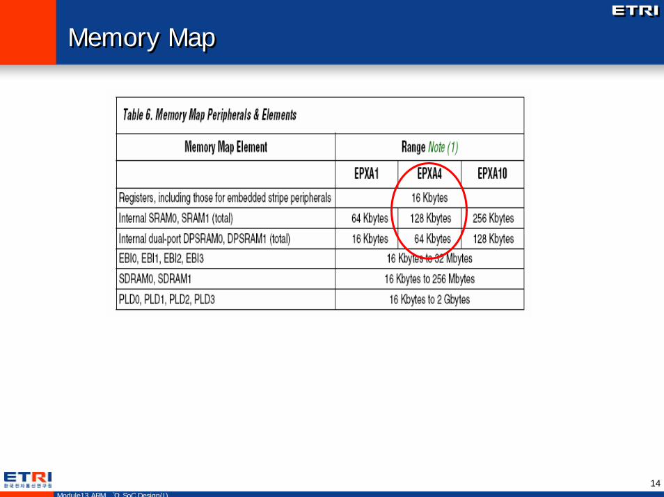
Memory Map Memory Map
15Module13 ARM기반 SoC Design(I)
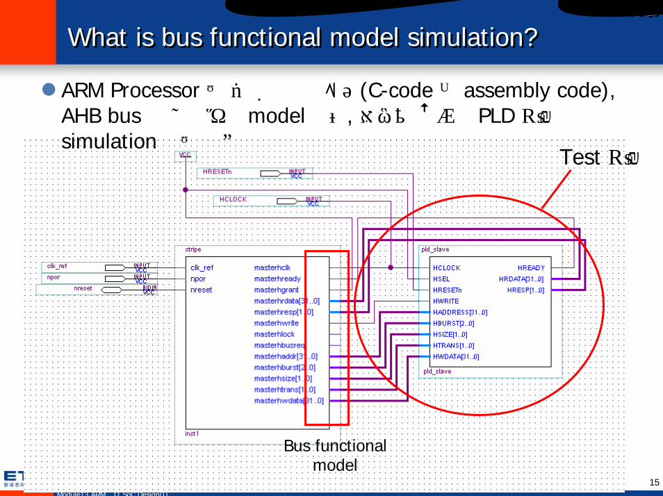
What is bus functional model simulation?What is bus functional model simulation?
ARM Processor 는 동작시키지 않고(C-code 나 assembly code), AHB bus 의 신호만을 model 하여, 우리가 설계한 PLD 부분을simulation 하는 방법
Test 부분
Bus functional model
16Module13 ARM기반 SoC Design(I)
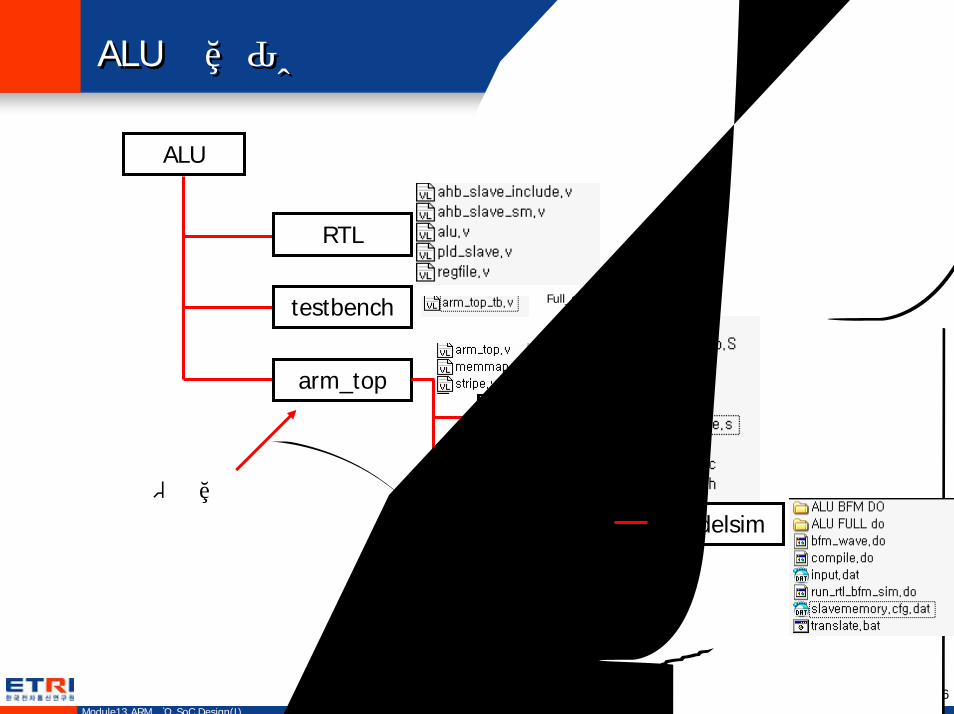
ALU 폴더 구성ALU 폴더 구성
ALU
RTL
testbench
arm_top
Full_stripe simulation시 사용
software
작업 폴더simulation modelsim
17Module13 ARM기반 SoC Design(I)
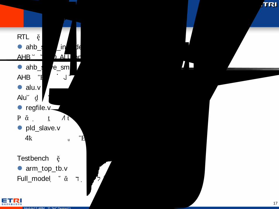
파일 설명파일 설명
RTL 폴더ahb_slave_include.v
AHB 에 신호과 ALU operations이 define 되있다. ahb_slave_sm.v
AHB 프로토콜 규약에 대해 신호 처리 부분이 코딩 되어있다.alu.v
Alu에 대한 로직이 있다.regfile.v
각 레지스터들의 어드레스 할당 밑 처리에 대해 코딩 되어있다
pld_slave.v위 4개 파일을 컴퍼넌트로 묶어 내는 TOP 모듈이다.
Testbench 폴더arm_top_tb.v
Full_model 시뮬레이션 시 사용되는 테스트 벤치 파일이다.
18Module13 ARM기반 SoC Design(I)
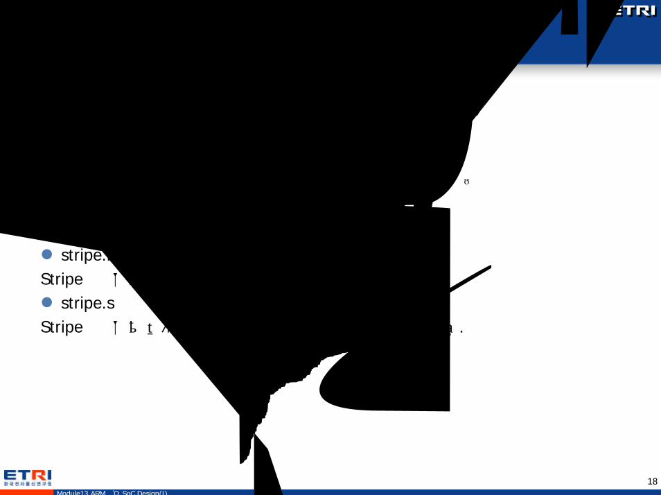
파일 설명파일 설명
Arm_top 폴더arm_top.v
전체 모듈에 대한 top파일이다. memmap.v
Stripe 과 PLD의 베이스 어드레스와 그 SIZE를 파라미터로 담고 있는 파일stripe.v
Maga-wizard에서 Stripe생성시 자동으로 생성되는 파일이다.stripe.h
Stripe의 정보가 들어있는 헤더 파일이다 C코드에서 참고한다.stripe.s
Stripe의 정보가 들어있는 헤더 파일이다 assem코드에서 참고한다.
19Module13 ARM기반 SoC Design(I)
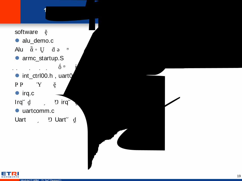
파일 설명파일 설명
software 폴더alu_demo.c
Alu의 연산등을 담고있는 펌웨어 파일이다. armc_startup.S
시스템 시작시 시작되는 코드로 arm을 셋팅하는 어셈 코드이다. int_ctrl00.h , uart00.h, uartcomm.h
각각의 이름의 헤더 파일이다.irq.c
Irq에대한 초기화와 irq에 대해 코딩 되어있다.uartcomm.c
Uart의 초기화와 Uart에 대해 코딩 되어있다.
20Module13 ARM기반 SoC Design(I)
프로젝트 설정하기프로젝트 설정하기
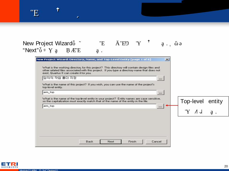
New Project Wizard를 실행해 프로젝트 경로와 이름을 설정한다. 그리고“Next”를눌러 다음 단계로 진행한다.
Top-level의entity
이름이어야 한다.
21Module13 ARM기반 SoC Design(I)
프로젝트 설정하기프로젝트 설정하기
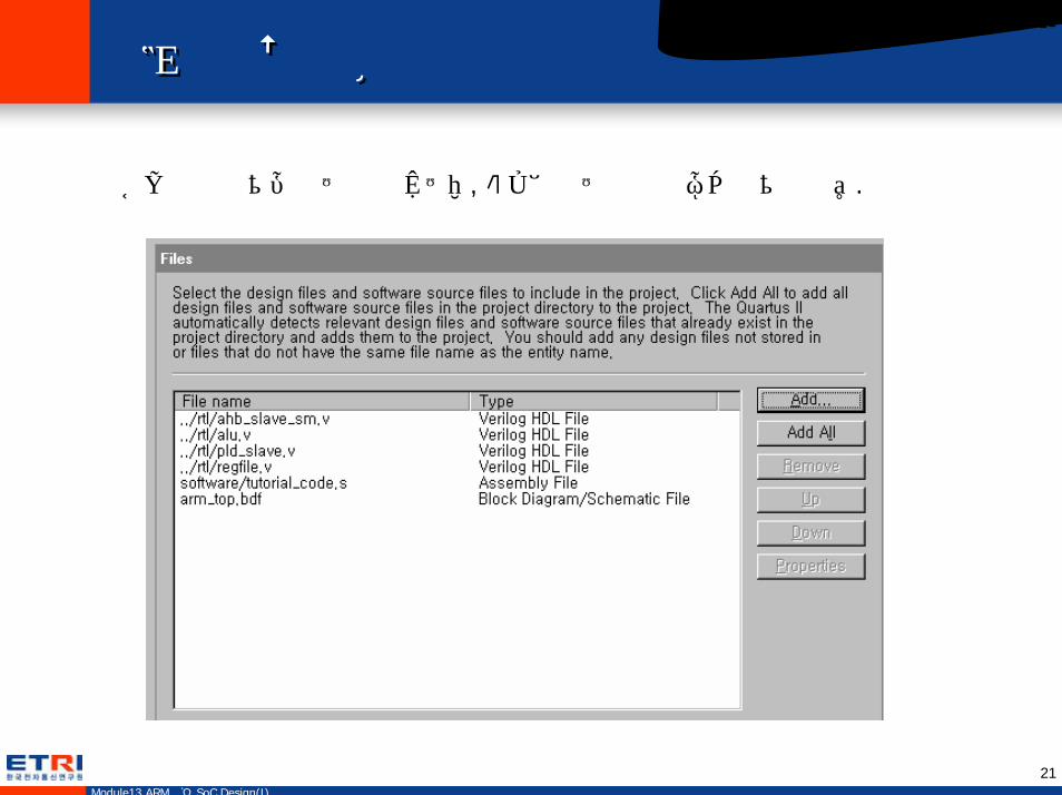
그럼 파일 추가를 하는 창이 뜨는데, 아래에 있는 파일을 모두 추가해 준다.
22Module13 ARM기반 SoC Design(I)
프로젝트 설정하기프로젝트 설정하기
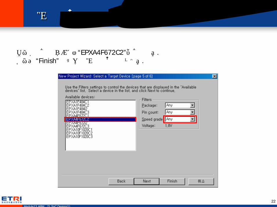
디바이스 선택 단계에서“EPXA4F672C2”를 선택한다.그리고 “Finish”을 눌러 프로젝트 설정을 끝낸다.
23Module13 ARM기반 SoC Design(I)
ARM Stripe 생성하기ARM Stripe 생성하기
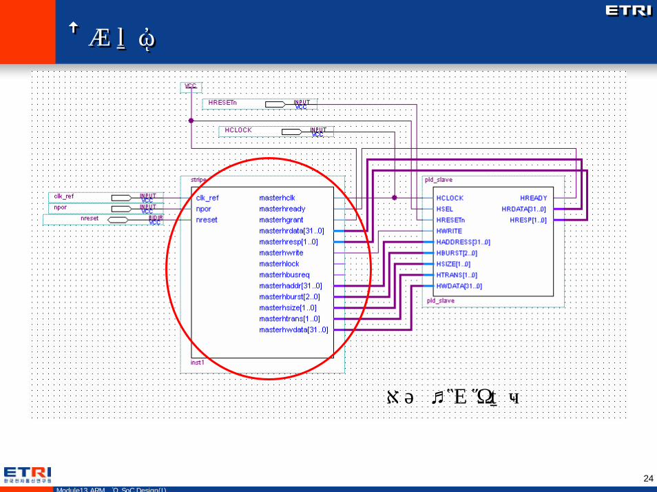
Top-level 설계 파일(arm_top.bdf)을 연다. 이 파일은 ARM Processor Stripe를 제외한 나머지 부분만 완성이 되어 있는 형태로 있다. 그래서 우리는ARM Stripe를 생성하므로 하드웨어 블록 설계를 완성할 수 있다. 다음그림은ARM Stripe만 빠져 있는 Top-level 설계 파일이다. ARM Stripe 심볼이 추가되어 있는 경우는 심볼을 삭제하고, stripe 생성 과정을 따라 한다.
TOOL => MEGA Wizard Plug-in
24Module13 ARM기반 SoC Design(I)
설계 도면설계 도면
지우고 새로 만들것
25Module13 ARM기반 SoC Design(I)
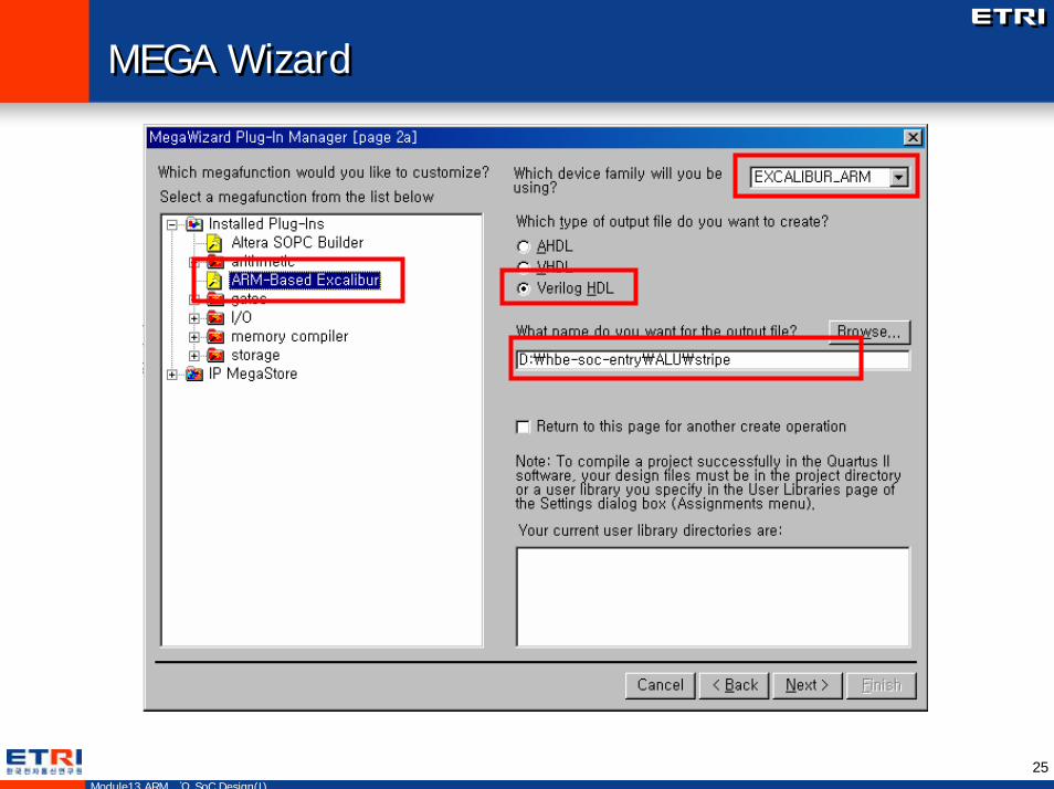
MEGA WizardMEGA Wizard
26Module13 ARM기반 SoC Design(I)
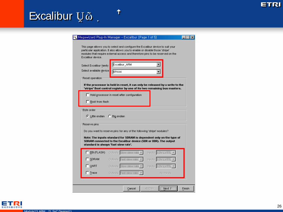
Excalibur 디바이스 설정Excalibur 디바이스 설정
27Module13 ARM기반 SoC Design(I)
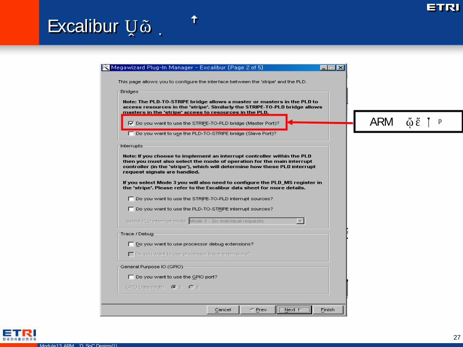
Excalibur 디바이스 설정Excalibur 디바이스 설정
ARM이 명령 보냄
28Module13 ARM기반 SoC Design(I)
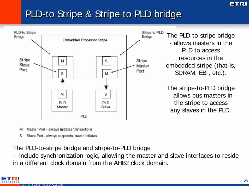
PLD-to Stripe & Stripe to PLD bridgePLD-to Stripe & Stripe to PLD bridge
The PLD-to-stripe bridge - allows masters in the
PLD to accessresources in the
embedded stripe (that is, SDRAM, EBI, etc.).
The stripe-to-PLD bridge - allows bus masters in
the stripe to accessany slaves in the PLD.
The PLD-to-stripe bridge and stripe-to-PLD bridge- include synchronization logic, allowing the master and slave interfaces to reside in a different clock domain from the AHB2 clock domain.
29Module13 ARM기반 SoC Design(I)
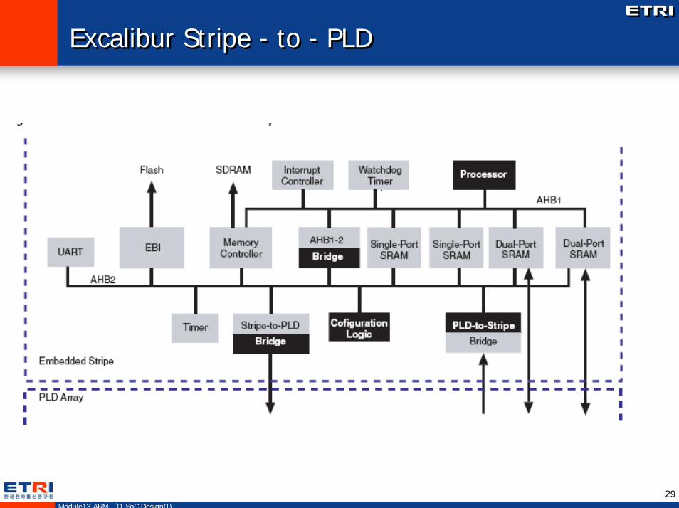
Excalibur Stripe - to - PLDExcalibur Stripe - to - PLD
30Module13 ARM기반 SoC Design(I)
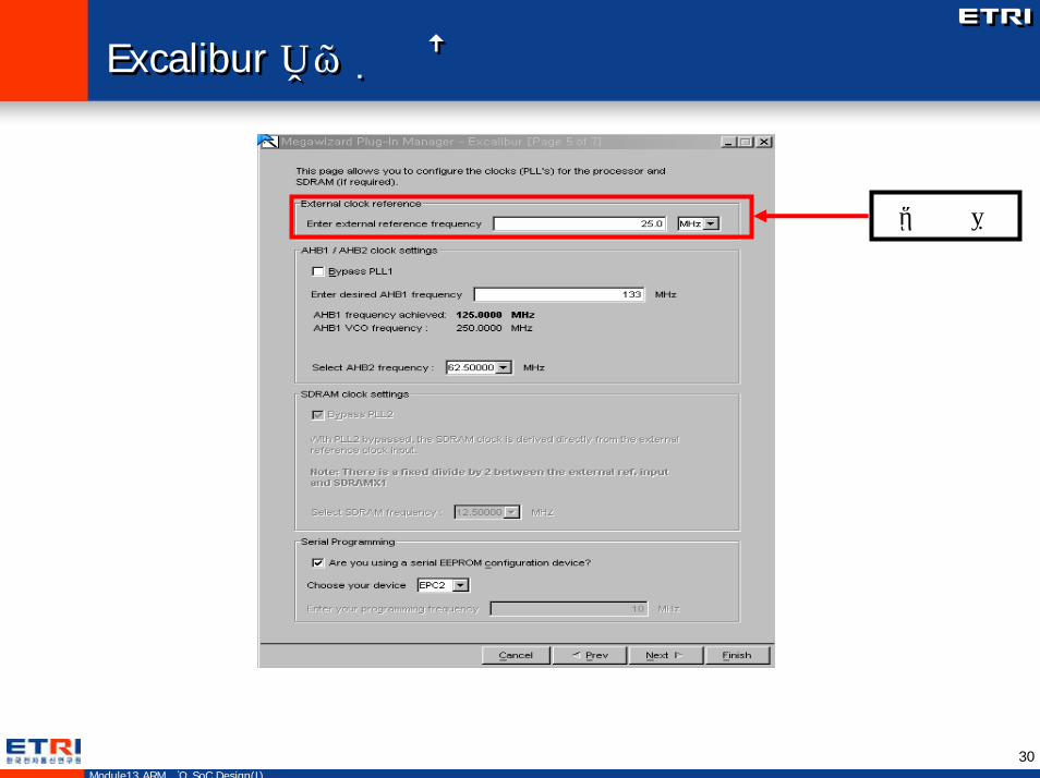
Excalibur 디바이스 설정Excalibur 디바이스 설정
메인 클럭
31Module13 ARM기반 SoC Design(I)
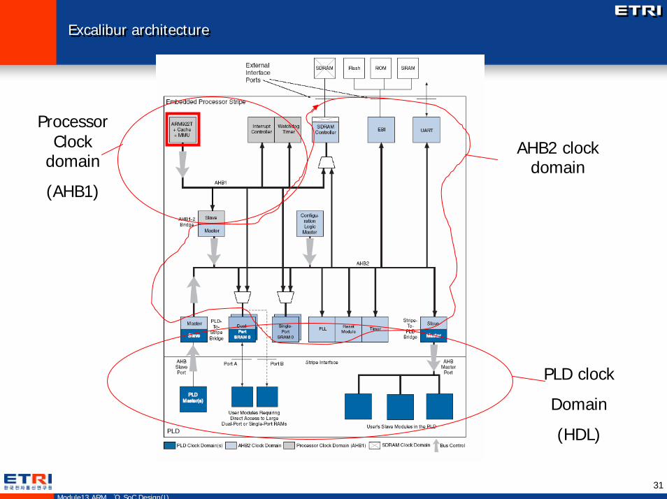
Excalibur architectureExcalibur architecture
ProcessorClock
domain
(AHB1)
PLD clock
Domain
(HDL)
AHB2 clock domain
32Module13 ARM기반 SoC Design(I)
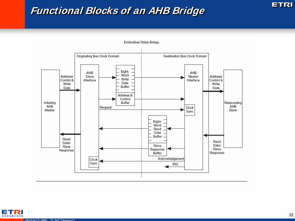
Functional Blocks of an AHB BridgeFunctional Blocks of an AHB Bridge

33Module13 ARM기반 SoC Design(I)
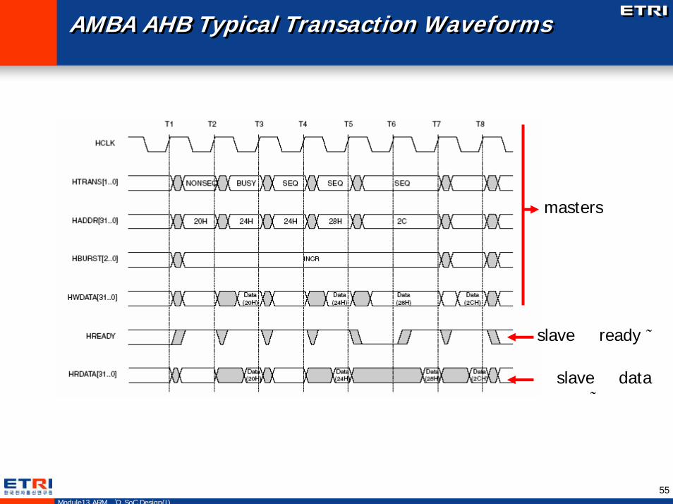
AMBA AHB Typical Transaction WaveformsAMBA AHB Typical Transaction Waveforms
slave 의 ready 신호
slave 의 data 신호
masters
34Module13 ARM기반 SoC Design(I)
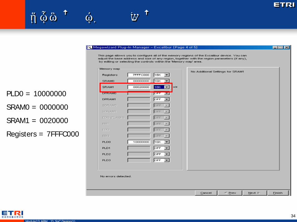
메모리 설정 밑 시작 주소 설정메모리 설정 밑 시작 주소 설정
PLD0 = 10000000
SRAM0 = 0000000
SRAM1 = 0020000
Registers = 7FFFC000
35Module13 ARM기반 SoC Design(I)
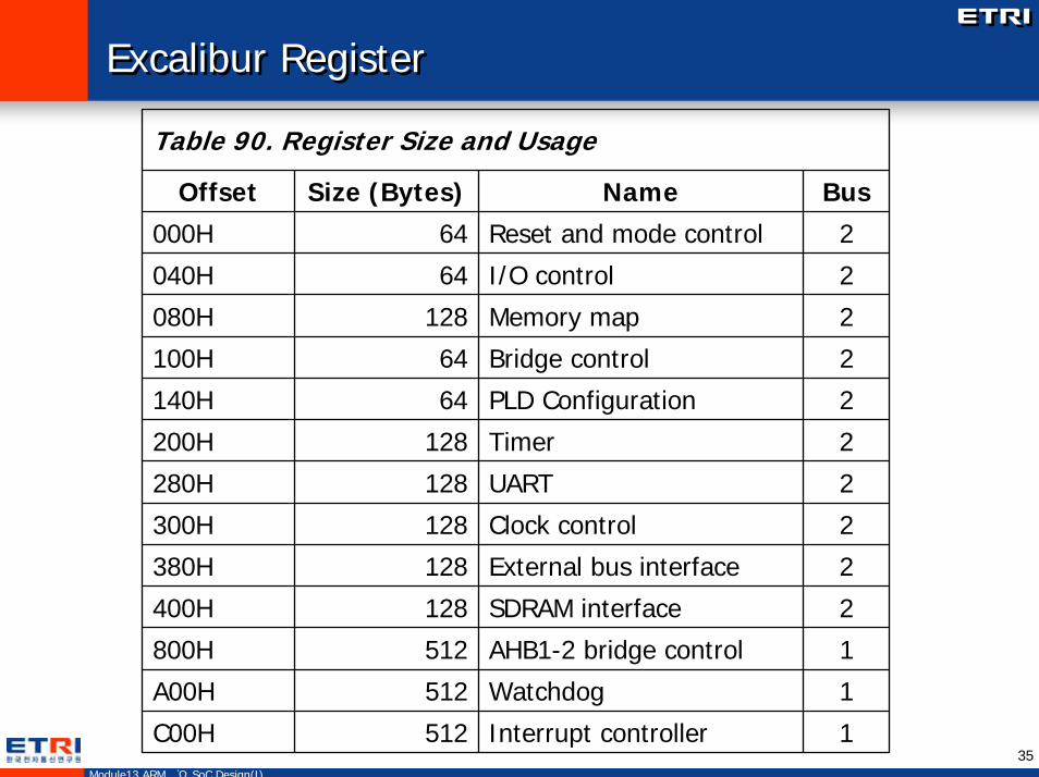
Excalibur Register Excalibur Register
Table 90. Register Size and Usage
Offset Size (Bytes) Name Bus
000H 64 Reset and mode control 2
040H 64 I/O control 2
080H 128 Memory map 2
100H 64 Bridge control 2
140H 64 PLD Configuration 2
200H 128 Timer 2
280H 128 UART 2
300H 128 Clock control 2
380H 128 External bus interface 2
400H 128 SDRAM interface 2
800H 512 AHB1-2 bridge control 1
A00H 512 Watchdog 1
C00H 512 Interrupt controller 1
36Module13 ARM기반 SoC Design(I)
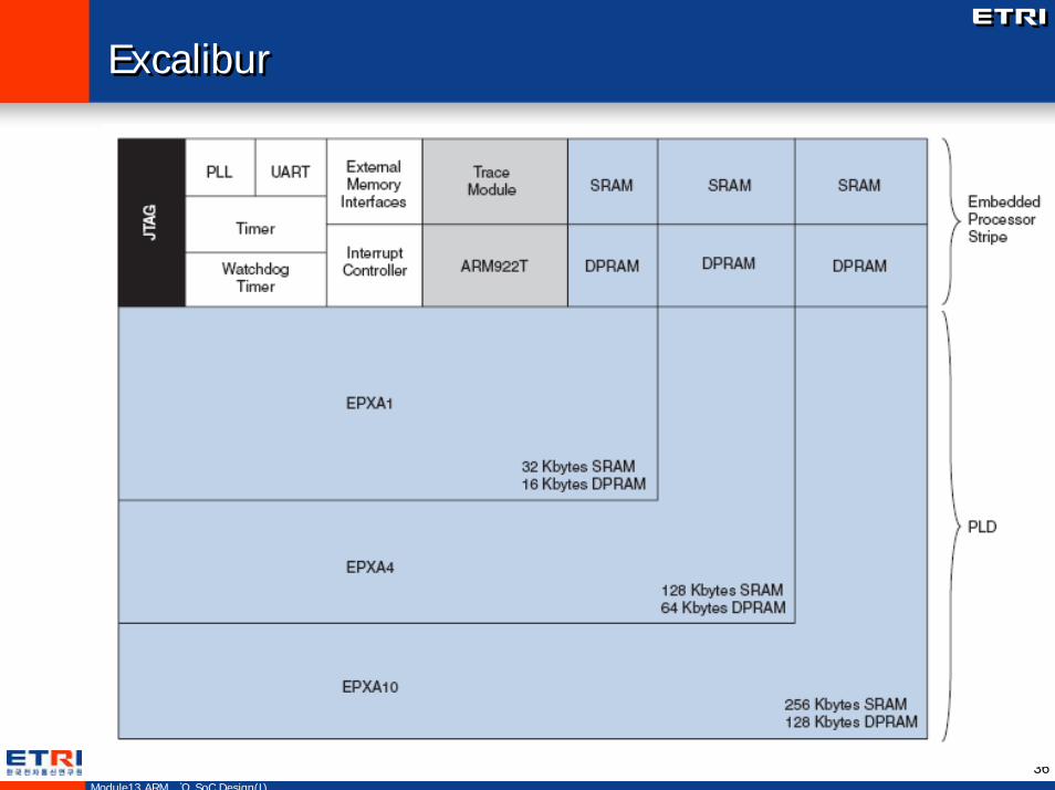
ExcaliburExcalibur
37Module13 ARM기반 SoC Design(I)
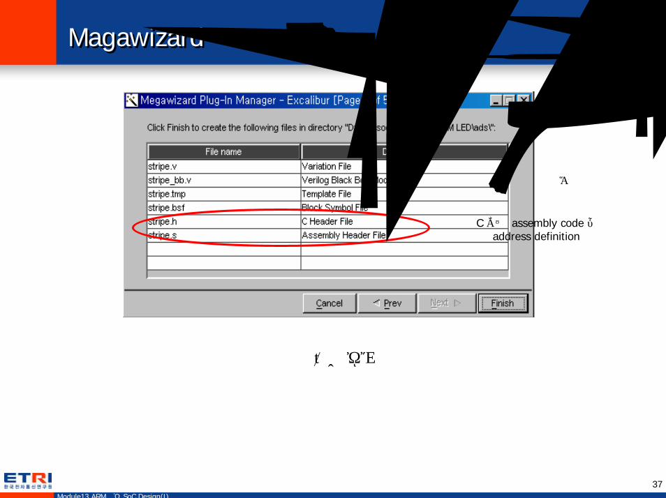
Magawizard 에서 생성되는 파일들Magawizard 에서 생성되는 파일들
합성을 위한 입출력 정의 파일
C 또는 assembly code 를 위한address definition 파일
파일 생성 목록
38Module13 ARM기반 SoC Design(I)
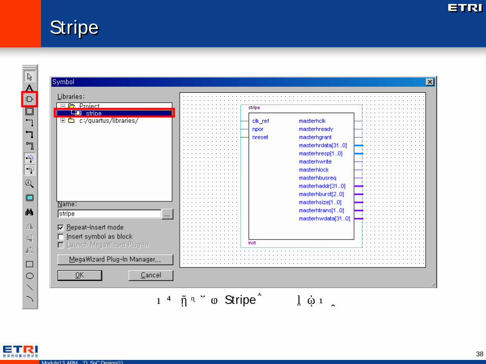
StripeStripe
심볼 메뉴에서 Stripe 선택 후 도면 완성
39Module13 ARM기반 SoC Design(I)
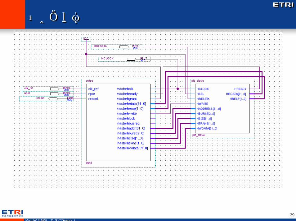
완성된 도면완성된 도면
40Module13 ARM기반 SoC Design(I)
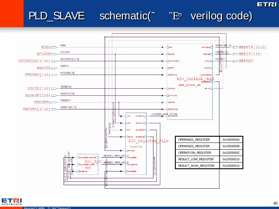
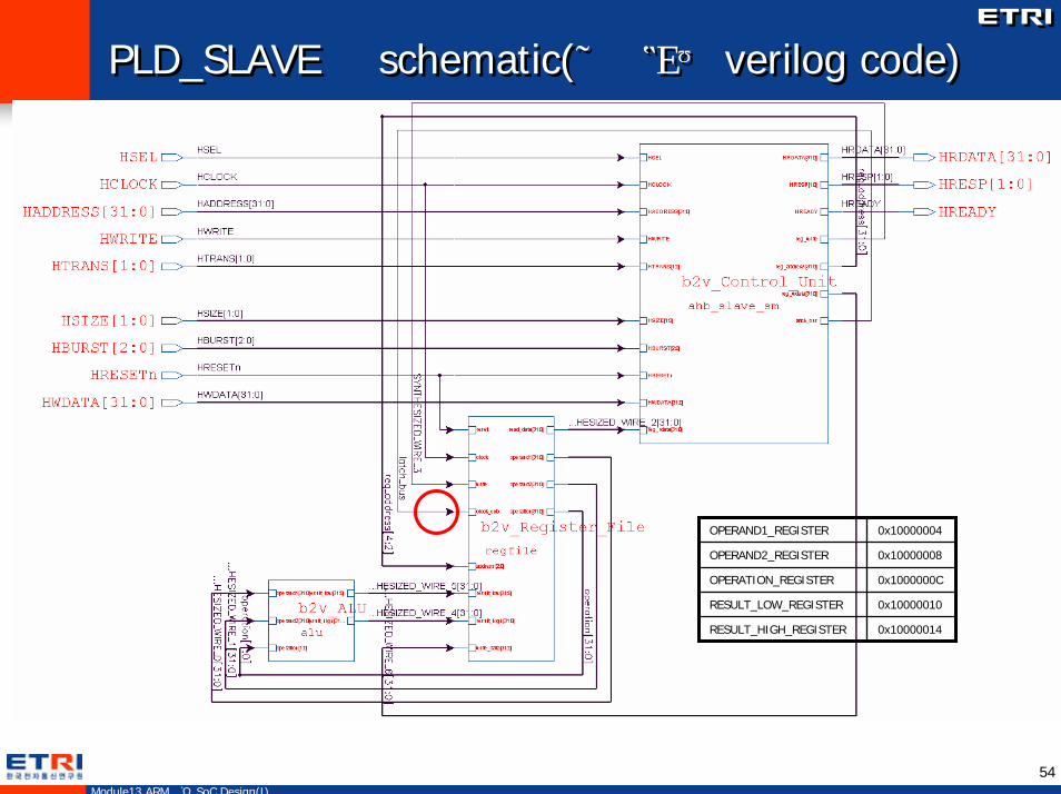
PLD_SLAVE 의 schematic(실제로는 verilog code) PLD_SLAVE 의 schematic(실제로는 verilog code)
OPERAND1_REGISTER 0x10000004
OPERAND2_REGISTER 0x10000008
OPERATION_REGISTER 0x1000000C
RESULT_LOW_REGISTER 0x10000010
RESULT_HIGH_REGISTER 0x10000014
41Module13 ARM기반 SoC Design(I)
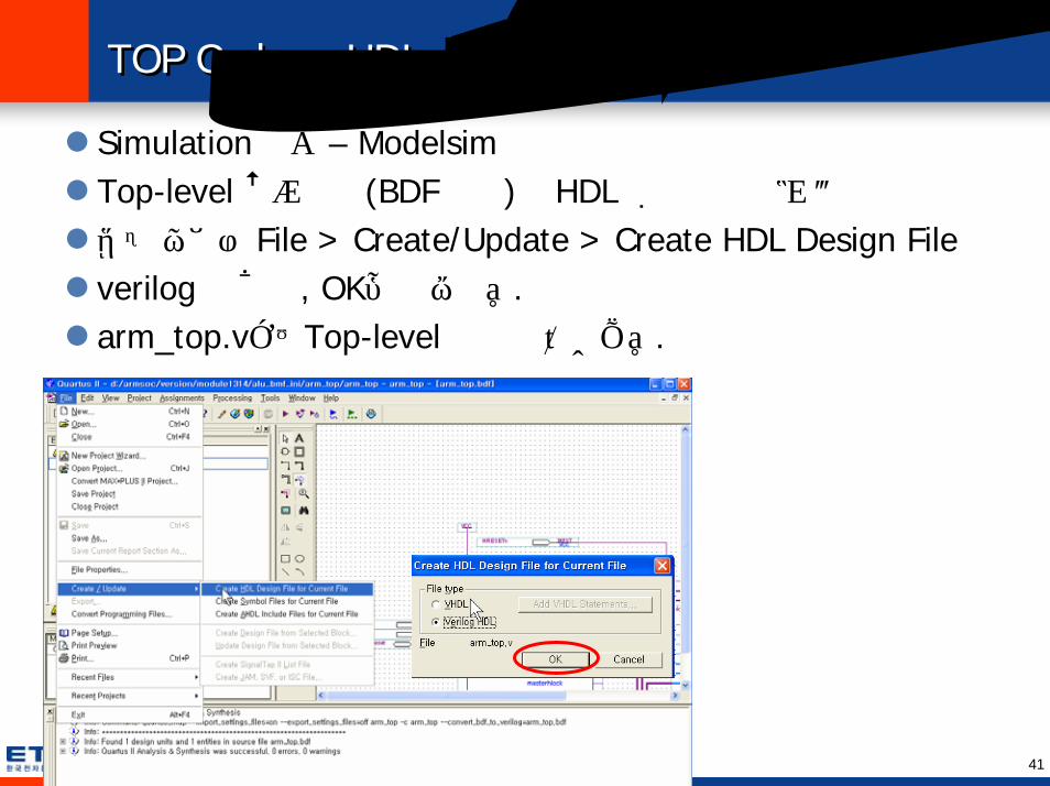
TOP Code 의 HDL 코드 생성TOP Code 의 HDL 코드 생성
Simulation 환경 – ModelsimTop-level 설계 파일(BDF 파일)을 HDL 형식의 파일로 변환메뉴 바에서 File > Create/Update > Create HDL Design File verilog 을 선택, OK를 클릭한다.arm_top.v라는Top-level 파일이 생성된다.
42Module13 ARM기반 SoC Design(I)
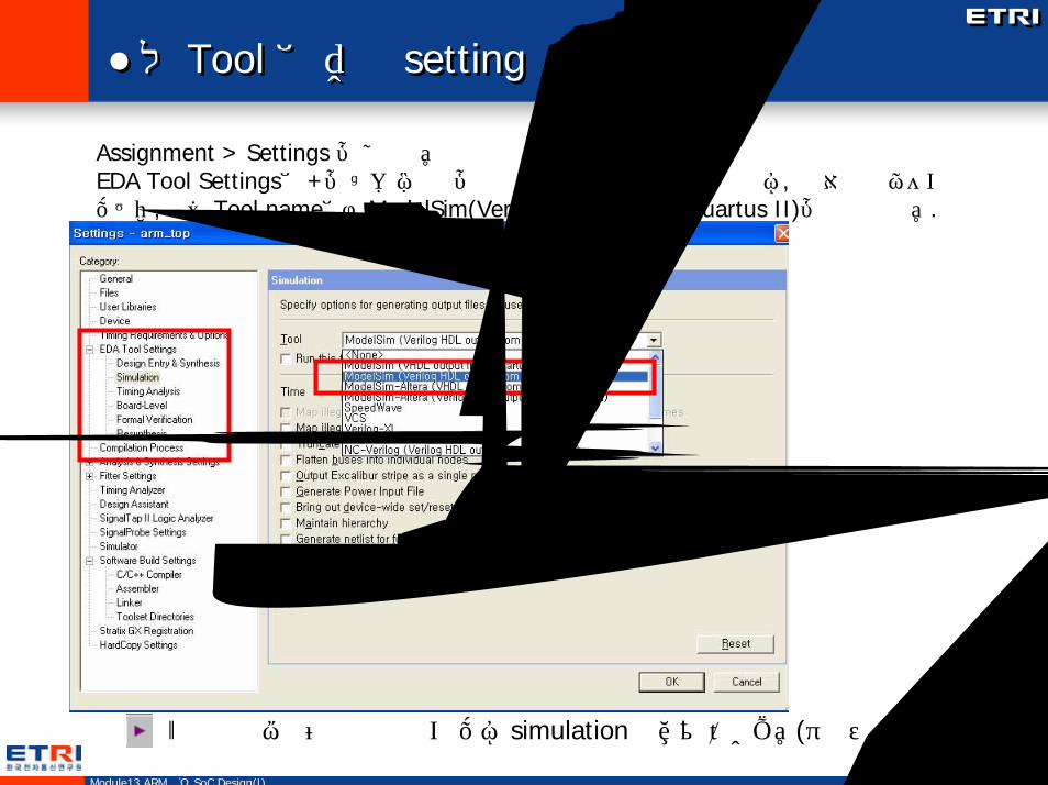
사용 Tool 에 대한 setting 사용 Tool 에 대한 setting
Assignment > Settings 를 실행한다EDA Tool Settings에 +를 눌러 리스트를 확장한 후 Simulation를 선택하면, 창 우측이 바뀌게되는데, 이때 Tool name에서 ModelSim(Verilog output from Quartus II)를 지정해 준다.
버튼을 클릭하여 컴파일 하게 되면 simulation 폴더가 생성된다(수행권장).
43Module13 ARM기반 SoC Design(I)
BFM(Bus Function Model) Functional Simulation을 위한 준비BFM(Bus Function Model) Functional Simulation을 위한 준비
시뮬레이션하기 위한 준비Bus 의 수행 모델 – input.datBus의 수행을 규정하는 형태로 바꿔야 함
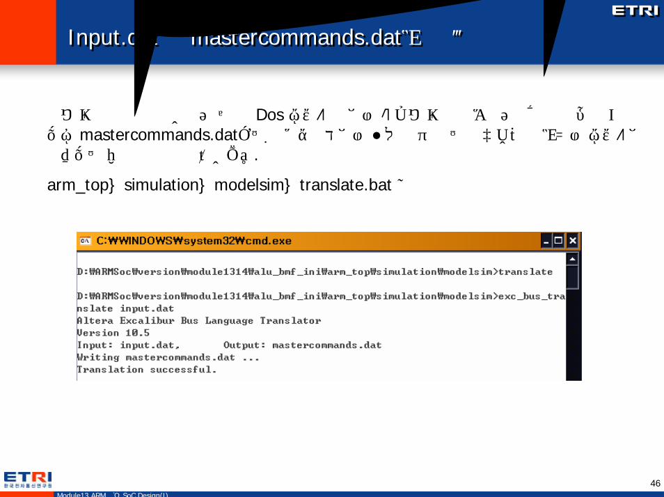
exc_bus_translate input.dat-> 출력결과 mastercommands.dat
altera_mf.vMastercommands.dat 파일을 사용해 stripe 의 시뮬레이션시파형 생성의 역할
44Module13 ARM기반 SoC Design(I)
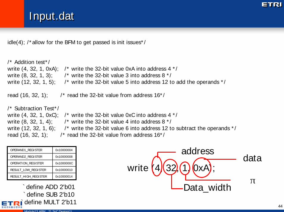
Input.datInput.dat
idle(4); /*allow for the BFM to get passed is init issues*/
/* Addition test*/write (4, 32, 1, 0xA); /* write the 32-bit value 0xA into address 4 */write (8, 32, 1, 3); /* write the 32-bit value 3 into address 8 */write (12, 32, 1, 5); /* write the 32-bit value 5 into address 12 to add the operands */
read (16, 32, 1); /* read the 32-bit value from address 16*/
/* Subtraction Test*/write (4, 32, 1, 0xC); /* write the 32-bit value 0xC into address 4 */write (8, 32, 1, 4); /* write the 32-bit value 4 into address 8 */write (12, 32, 1, 6); /* write the 32-bit value 6 into address 12 to subtract the operands */read (16, 32, 1); /* read the 32-bit value from address 16*/
OPERAND1_REGISTER 0x10000004
OPERAND2_REGISTER 0x10000008
OPERATION_REGISTER 0x1000000C
RESULT_LOW_REGISTER 0x10000010
RESULT_HIGH_REGISTER 0x10000014
address
write (4, 32, 1, 0xA);
Data_width횟수
data
`define ADD 2'b01`define SUB 2'b10
`define MULT 2'b11
45Module13 ARM기반 SoC Design(I)
Input.datInput.dat
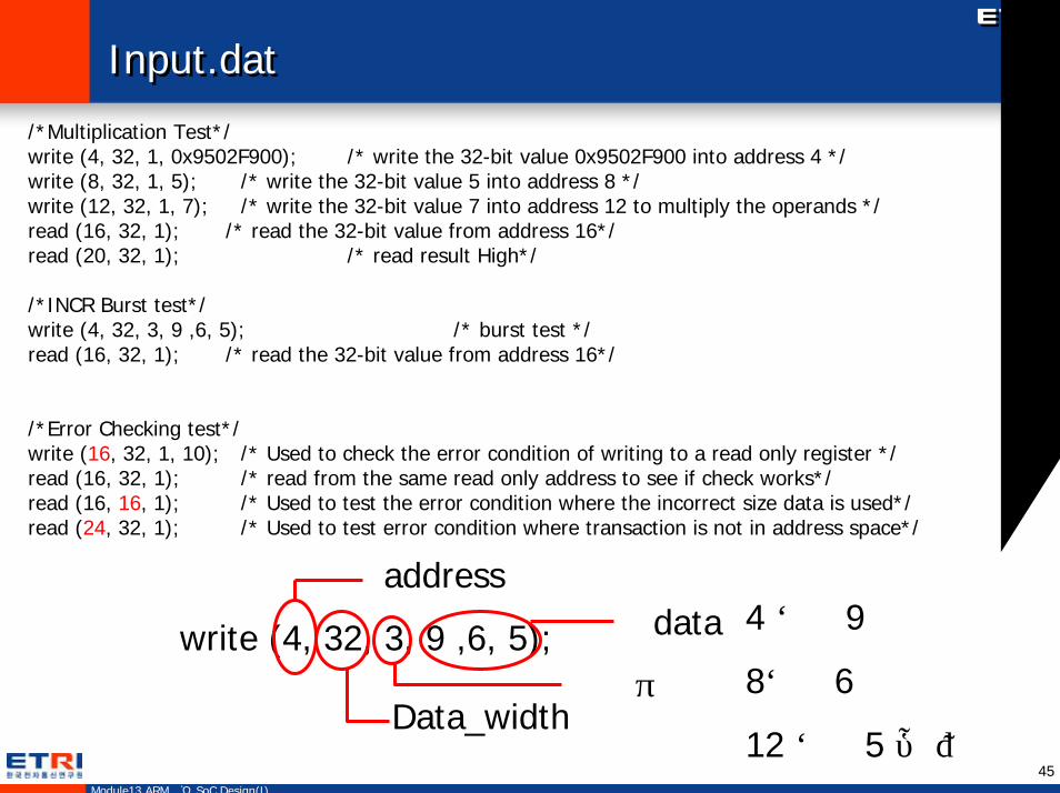
/*Multiplication Test*/write (4, 32, 1, 0x9502F900); /* write the 32-bit value 0x9502F900 into address 4 */write (8, 32, 1, 5); /* write the 32-bit value 5 into address 8 */write (12, 32, 1, 7); /* write the 32-bit value 7 into address 12 to multiply the operands */read (16, 32, 1); /* read the 32-bit value from address 16*/read (20, 32, 1); /* read result High*/
/*INCR Burst test*/write (4, 32, 3, 9 ,6, 5); /* burst test */read (16, 32, 1); /* read the 32-bit value from address 16*/
/*Error Checking test*/write (16, 32, 1, 10); /* Used to check the error condition of writing to a read only register */read (16, 32, 1); /* read from the same read only address to see if check works*/read (16, 16, 1); /* Used to test the error condition where the incorrect size data is used*/read (24, 32, 1); /* Used to test error condition where transaction is not in address space*/
address
write (4, 32, 3, 9 ,6, 5);
Data_width횟수
data 4 번지 9
8번지 6
12 번지 5 를 넣음
46Module13 ARM기반 SoC Design(I)
Input.dat 의 mastercommands.dat로의 변환Input.dat 의 mastercommands.dat로의 변환
위와 같이 파일을 작성하고 난 후 Dos 명령어 창에서 아래와 같이 입력하고 엔터 키를 치게되면 mastercommands.dat라는 시뮬레이션에서 사용할 수 있는 임베디드 프로세서 명령어에해당되는 데이터 파일이 생성된다.
arm_top₩simulation₩modelsim₩translate.bat 실행
47Module13 ARM기반 SoC Design(I)
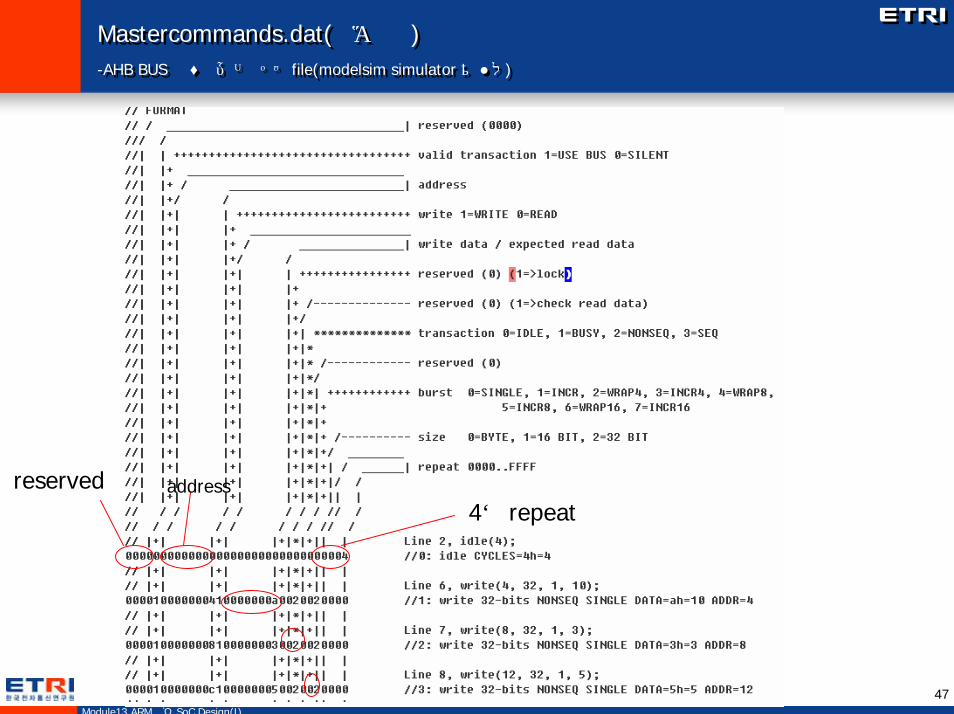
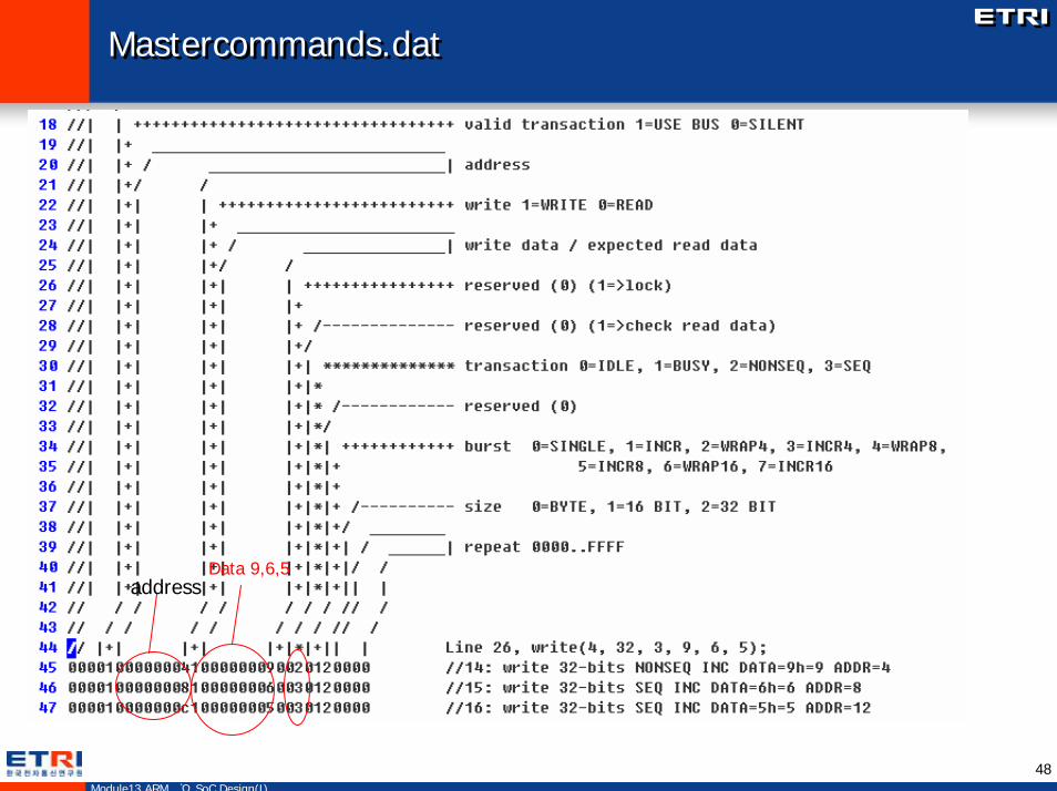
Mastercommands.dat(출력파일)-AHB BUS 의 상태를 나타내는 file(modelsim simulator 가 사용)
Mastercommands.dat(출력파일)-AHB BUS 의 상태를 나타내는 file(modelsim simulator 가 사용)
reserved address4번 repeat
48Module13 ARM기반 SoC Design(I)
Mastercommands.datMastercommands.dat
addressData 9,6,5
49Module13 ARM기반 SoC Design(I)
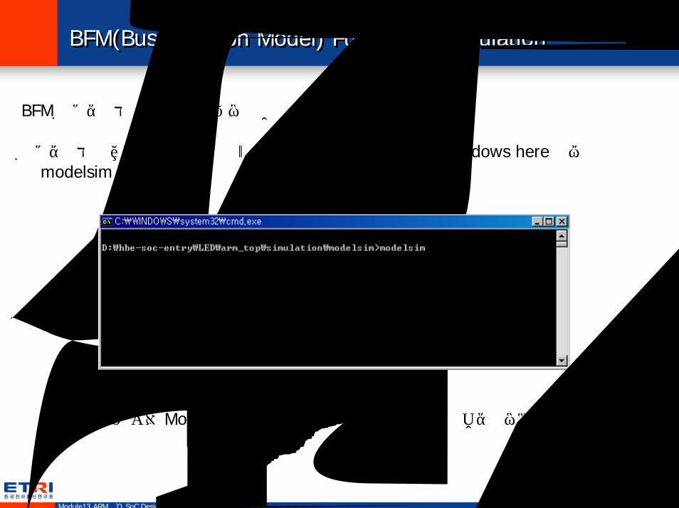
BFM(Bus Function Model) Functional SimulationBFM(Bus Function Model) Functional Simulation
BFM 시뮬레이션을 하기 위해 미리 작성한 Compile.do 파일 사용
시뮬레이션 폴더에 마우스 오른쪽 버튼 클릭 후 open command windows here 클릭후 modelsim 실행
위 방법이 안될 경우 Modelsim 실행 후 시뮬레이션 폴더를 체인지 디렉토리로 잡는다.
50Module13 ARM기반 SoC Design(I)
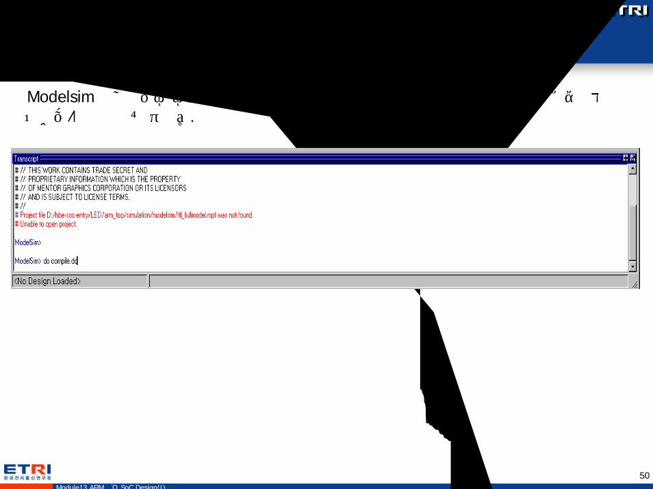
BFM(Bus Function Model) Functional SimulationBFM(Bus Function Model) Functional Simulation
Modelsim이 실행되면 명령어 창에 do compile.do 입력 하면 자동으로 컴파일과 시뮬레이션이완성되어 파형을 볼 수있다.

51Module13 ARM기반 SoC Design(I)
Compile.do 파일Compile.do 파일
vlib work
vlog ../../stripe.v# maga wizard 에서 생성시킨 파일vlog +incdir+../../../rtl ../../../rtl/regfile.vvlog +incdir+../../../rtl ../../../rtl/alu.vvlog +incdir+../../../rtl ../../../rtl/pld_slave.vvlog +incdir+../../../rtl ../../../rtl/ahb_slave_sm.vvlog ../../arm_top.v# schematic editor 에서 생성한 top 파일
vlog C:/quartus/eda/sim_lib/excalibur/lpm/ALT_EXC_STRIPE_BFM.V# stripe 의 bus functional model vlog C:/quartus/eda/sim_lib/altera_mf.v# altera mega function library #이 파일에서 생성된 mastercommands.dat 파일을 읽어냄.
vsim arm_toplog -r /*view wave do bfm_wave.do # wave 창에 trace 된 신호를 보자do run_rtl_bfm_sim.do # arm_top에 입력 signal 을 drive 하는 파일
52Module13 ARM기반 SoC Design(I)
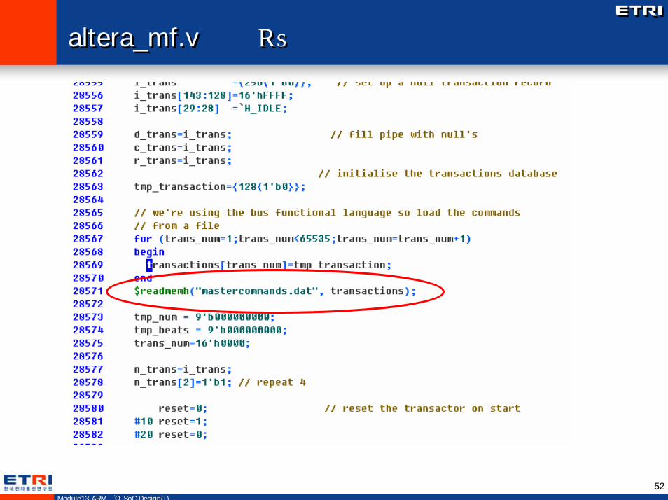
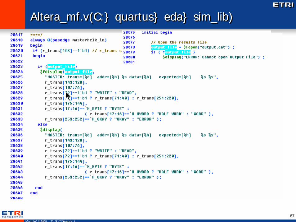
altera_mf.v 의 일부altera_mf.v 의 일부
53Module13 ARM기반 SoC Design(I)
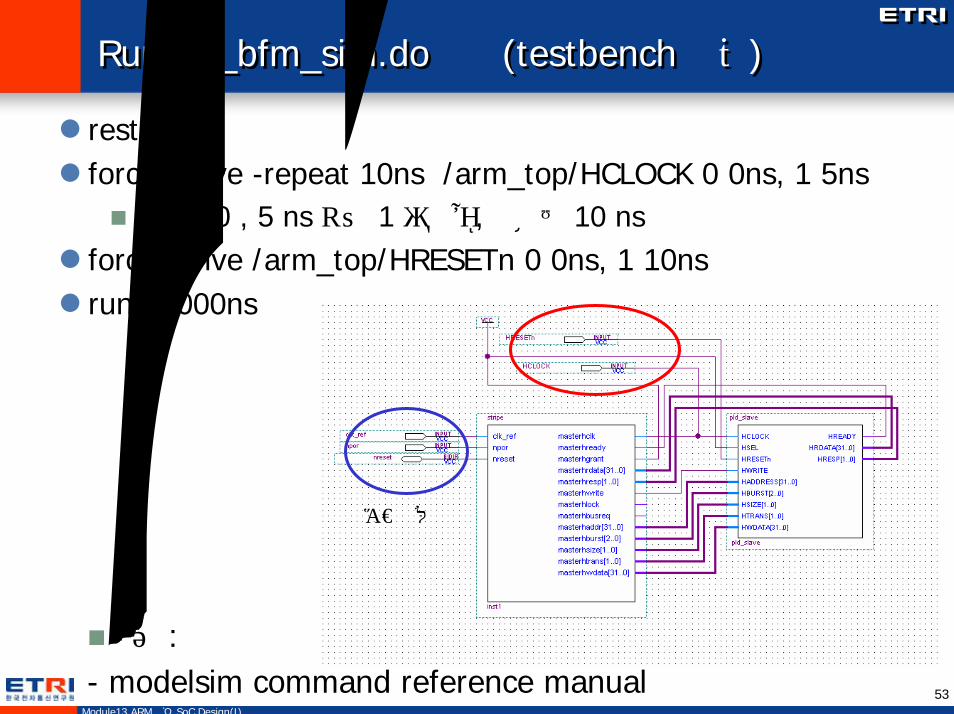
Run_rtl_bfm_sim.do 파일(testbench 코드) Run_rtl_bfm_sim.do 파일(testbench 코드)
restart -fforce -drive -repeat 10ns /arm_top/HCLOCK 0 0ns, 1 5ns초기값 0 , 5 ns 부터 1 값이며, 주기는 10 ns
force -drive /arm_top/HRESETn 0 0ns, 1 10nsrun 14000ns
참고 : - modelsim command reference manual
입력불필요
54Module13 ARM기반 SoC Design(I)
PLD_SLAVE 의 schematic(실제로는 verilog code) PLD_SLAVE 의 schematic(실제로는 verilog code)
OPERAND1_REGISTER 0x10000004
OPERAND2_REGISTER 0x10000008
OPERATION_REGISTER 0x1000000C
RESULT_LOW_REGISTER 0x10000010
RESULT_HIGH_REGISTER 0x10000014
55Module13 ARM기반 SoC Design(I)
AMBA AHB Typical Transaction WaveformsAMBA AHB Typical Transaction Waveforms
slave 의 ready 신호
slave 의 data 신호
masters
56Module13 ARM기반 SoC Design(I)
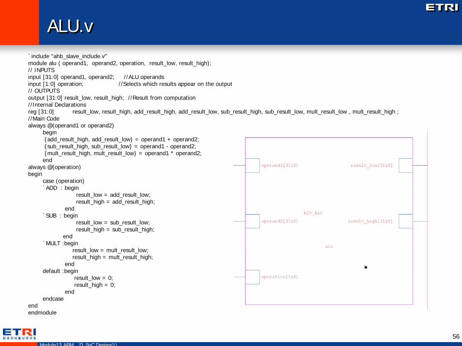
ALU.vALU.v`include "ahb_slave_include.v"module alu ( operand1, operand2, operation, result_low, result_high);// INPUTSinput [31:0] operand1, operand2; //ALU operandsinput [1:0] operation; //Selects which results appear on the output// OUTPUTSoutput [31:0] result_low, result_high; //Result from computation//Internal Declarationsreg [31:0] result_low, result_high, add_result_high, add_result_low, sub_result_high, sub_result_low, mult_result_low , mult_result_high ;//Main Codealways @(operand1 or operand2)
begin{add_result_high, add_result_low} = operand1 + operand2;{sub_result_high, sub_result_low} = operand1 - operand2;{mult_result_high, mult_result_low} = operand1 * operand2;
endalways @(operation)begin
case (operation)`ADD : begin
result_low = add_result_low;result_high = add_result_high;
end`SUB : begin
result_low = sub_result_low;result_high = sub_result_high;
end`MULT :begin
result_low = mult_result_low;result_high = mult_result_high;
enddefault :begin
result_low = 0;result_high = 0;
endendcase
endendmodule
57Module13 ARM기반 SoC Design(I)
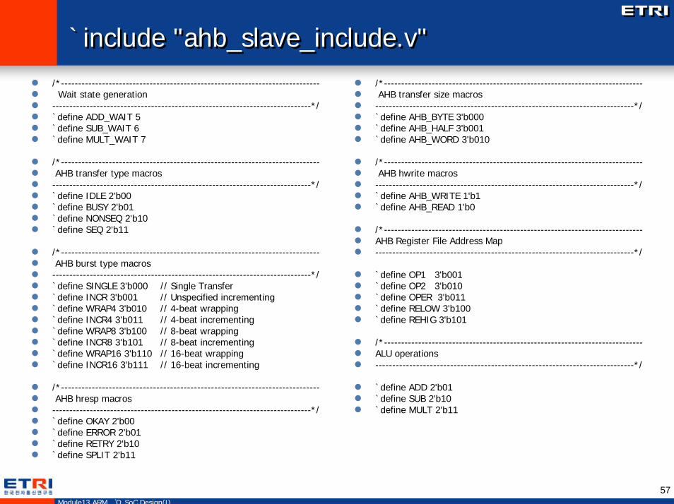
`include "ahb_slave_include.v"`include "ahb_slave_include.v"/*----------------------------------------------------------------------------AHB transfer size macros----------------------------------------------------------------------------*/`define AHB_BYTE 3'b000`define AHB_HALF 3'b001`define AHB_WORD 3'b010
/*----------------------------------------------------------------------------AHB hwrite macros----------------------------------------------------------------------------*/`define AHB_WRITE 1'b1`define AHB_READ 1'b0
/*----------------------------------------------------------------------------AHB Register File Address Map----------------------------------------------------------------------------*/
`define OP1 3'b001`define OP2 3'b010`define OPER 3'b011`define RELOW 3'b100`define REHIG 3'b101
/*----------------------------------------------------------------------------ALU operations----------------------------------------------------------------------------*/
`define ADD 2'b01`define SUB 2'b10`define MULT 2'b11
/*----------------------------------------------------------------------------Wait state generation
----------------------------------------------------------------------------*/`define ADD_WAIT 5`define SUB_WAIT 6`define MULT_WAIT 7
/*----------------------------------------------------------------------------AHB transfer type macros----------------------------------------------------------------------------*/`define IDLE 2'b00`define BUSY 2'b01`define NONSEQ 2'b10`define SEQ 2'b11
/*----------------------------------------------------------------------------AHB burst type macros----------------------------------------------------------------------------*/`define SINGLE 3'b000 // Single Transfer`define INCR 3'b001 // Unspecified incrementing`define WRAP4 3'b010 // 4-beat wrapping`define INCR4 3'b011 // 4-beat incrementing`define WRAP8 3'b100 // 8-beat wrapping`define INCR8 3'b101 // 8-beat incrementing`define WRAP16 3'b110 // 16-beat wrapping`define INCR16 3'b111 // 16-beat incrementing
/*----------------------------------------------------------------------------AHB hresp macros----------------------------------------------------------------------------*/`define OKAY 2'b00`define ERROR 2'b01`define RETRY 2'b10`define SPLIT 2'b11
58Module13 ARM기반 SoC Design(I)
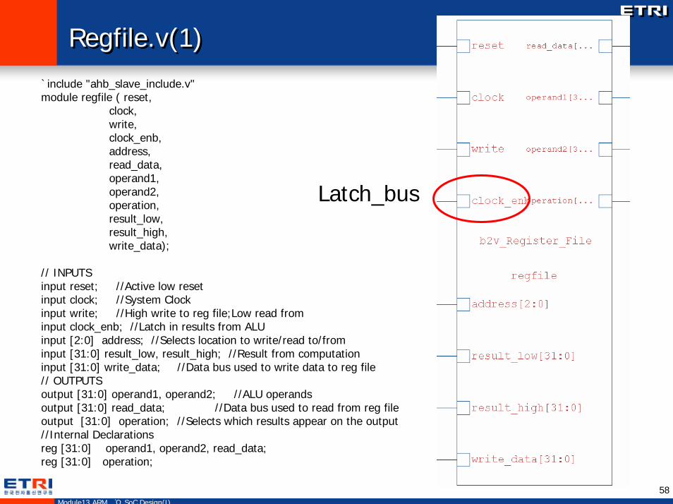
Regfile.v(1)Regfile.v(1)
`include "ahb_slave_include.v"module regfile ( reset,
clock,write,clock_enb,address,read_data,operand1, operand2,operation,result_low,result_high,write_data);
// INPUTSinput reset; //Active low resetinput clock; //System Clock input write; //High write to reg file;Low read frominput clock_enb; //Latch in results from ALUinput [2:0] address; //Selects location to write/read to/frominput [31:0] result_low, result_high; //Result from computationinput [31:0] write_data; //Data bus used to write data to reg file// OUTPUTSoutput [31:0] operand1, operand2; //ALU operandsoutput [31:0] read_data; //Data bus used to read from reg fileoutput [31:0] operation; //Selects which results appear on the output//Internal Declarationsreg [31:0] operand1, operand2, read_data;reg [31:0] operation;
Latch_bus
59Module13 ARM기반 SoC Design(I)
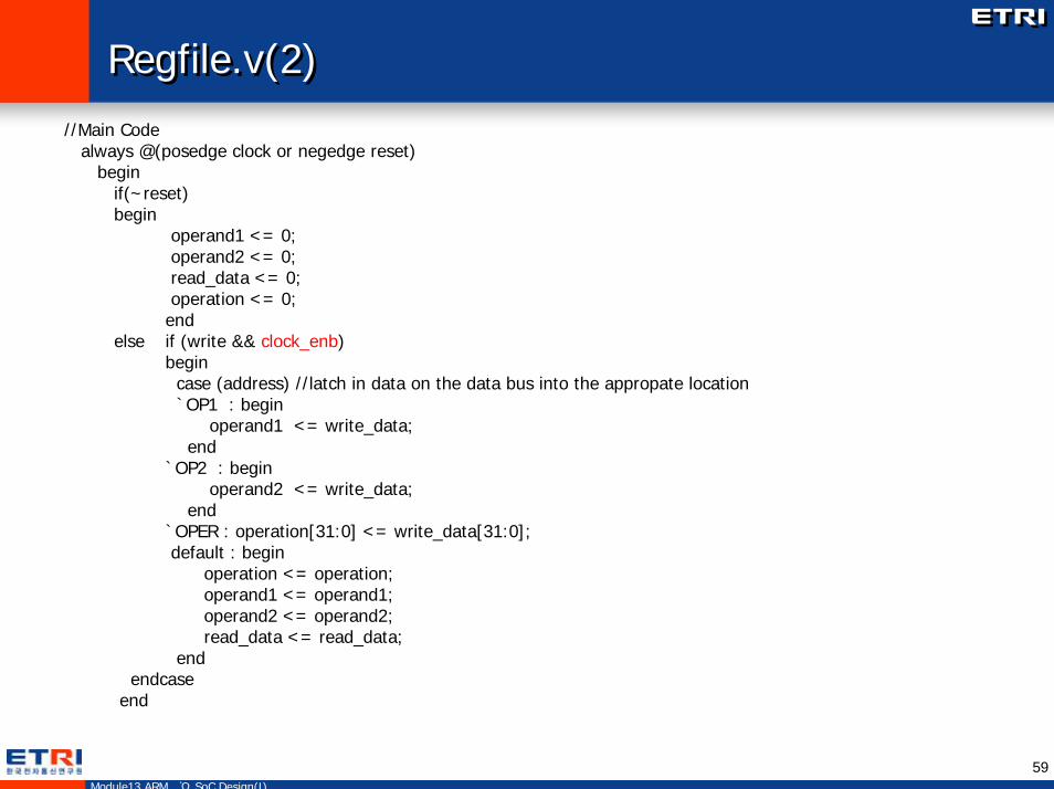
Regfile.v(2)Regfile.v(2)//Main Code
always @(posedge clock or negedge reset)begin
if(~reset)begin
operand1 <= 0;operand2 <= 0; read_data <= 0;operation <= 0;
endelse if (write && clock_enb)
begincase (address) //latch in data on the data bus into the appropate location`OP1 : begin
operand1 <= write_data;end
`OP2 : beginoperand2 <= write_data;
end`OPER : operation[31:0] <= write_data[31:0];default : begin
operation <= operation;operand1 <= operand1;operand2 <= operand2;read_data <= read_data;
endendcase
end
60Module13 ARM기반 SoC Design(I)
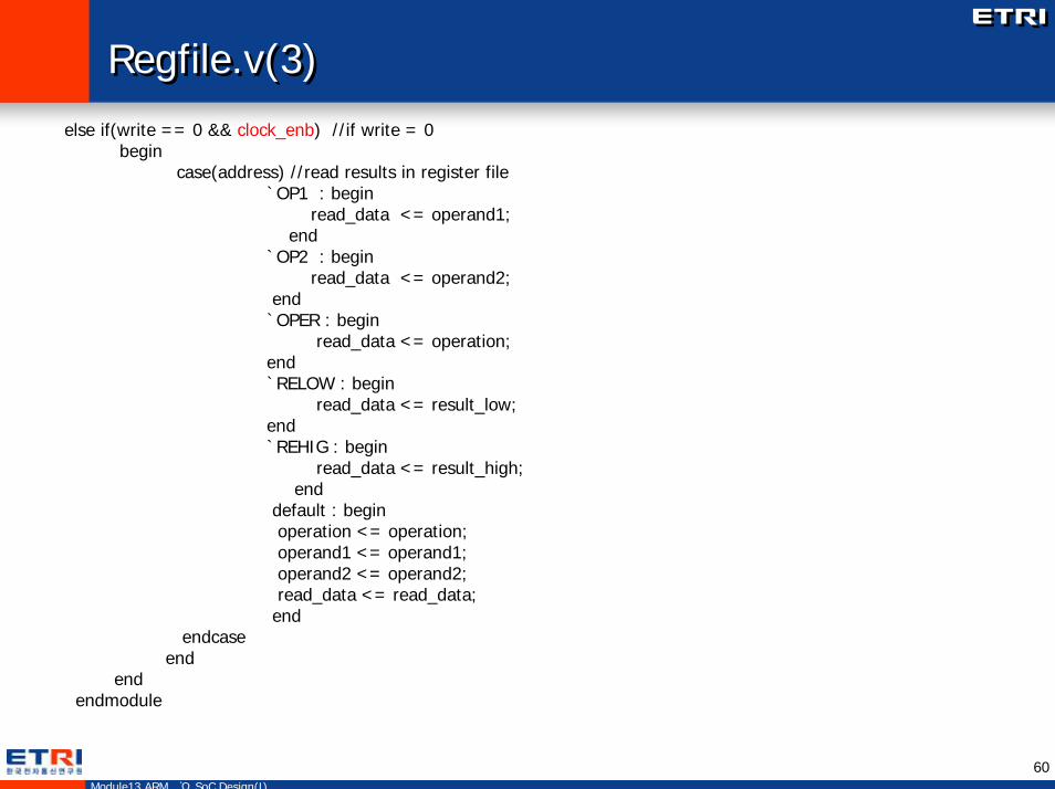
Regfile.v(3)Regfile.v(3)else if(write == 0 && clock_enb) //if write = 0
begincase(address) //read results in register file
`OP1 : beginread_data <= operand1;
end`OP2 : begin
read_data <= operand2;end
`OPER : beginread_data <= operation;
end`RELOW : begin
read_data <= result_low;end`REHIG : begin
read_data <= result_high;end
default : beginoperation <= operation;operand1 <= operand1;operand2 <= operand2;read_data <= read_data;
endendcase
endend
endmodule
61Module13 ARM기반 SoC Design(I)
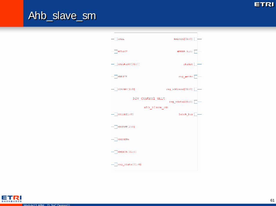
Ahb_slave_smAhb_slave_sm
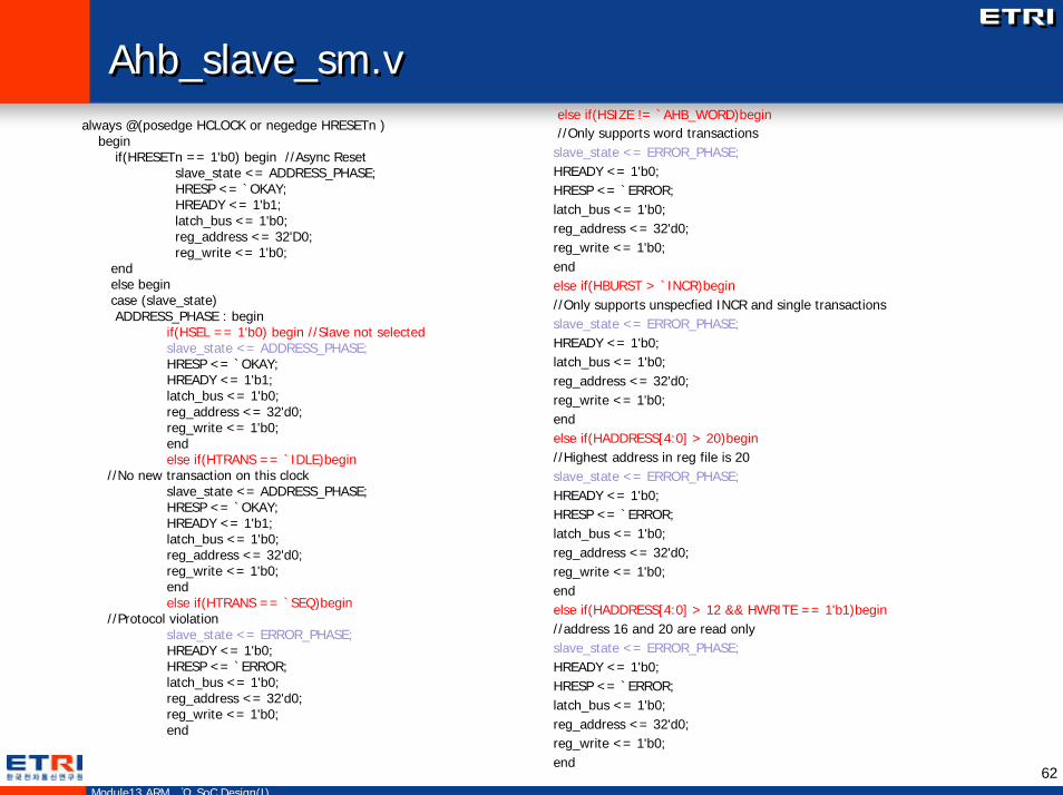
62Module13 ARM기반 SoC Design(I)
Ahb_slave_sm.vAhb_slave_sm.v
else if(HSIZE != `AHB_WORD)begin//Only supports word transactions
slave_state <= ERROR_PHASE;HREADY <= 1'b0;HRESP <= `ERROR;latch_bus <= 1'b0;reg_address <= 32'd0;reg_write <= 1'b0; endelse if(HBURST > `INCR)begin//Only supports unspecfied INCR and single transactionsslave_state <= ERROR_PHASE;HREADY <= 1'b0;latch_bus <= 1'b0;reg_address <= 32'd0;reg_write <= 1'b0; endelse if(HADDRESS[4:0] > 20)begin//Highest address in reg file is 20slave_state <= ERROR_PHASE;HREADY <= 1'b0;HRESP <= `ERROR;latch_bus <= 1'b0;reg_address <= 32'd0;reg_write <= 1'b0; endelse if(HADDRESS[4:0] > 12 && HWRITE == 1'b1)begin//address 16 and 20 are read onlyslave_state <= ERROR_PHASE;HREADY <= 1'b0;HRESP <= `ERROR;latch_bus <= 1'b0;reg_address <= 32'd0;reg_write <= 1'b0;
always @(posedge HCLOCK or negedge HRESETn )begin
if(HRESETn == 1'b0) begin //Async Resetslave_state <= ADDRESS_PHASE;HRESP <= `OKAY;HREADY <= 1'b1;latch_bus <= 1'b0;reg_address <= 32'D0;reg_write <= 1'b0;
endelse begincase (slave_state)ADDRESS_PHASE : begin
if(HSEL == 1'b0) begin //Slave not selectedslave_state <= ADDRESS_PHASE;HRESP <= `OKAY;HREADY <= 1'b1;latch_bus <= 1'b0;reg_address <= 32'd0;reg_write <= 1'b0; end else if(HTRANS == `IDLE)begin
//No new transaction on this clockslave_state <= ADDRESS_PHASE;HRESP <= `OKAY;HREADY <= 1'b1;latch_bus <= 1'b0;reg_address <= 32'd0;reg_write <= 1'b0; endelse if(HTRANS == `SEQ)begin
//Protocol violationslave_state <= ERROR_PHASE;HREADY <= 1'b0;HRESP <= `ERROR;latch_bus <= 1'b0;reg_address <= 32'd0;reg_write <= 1'b0; end
end
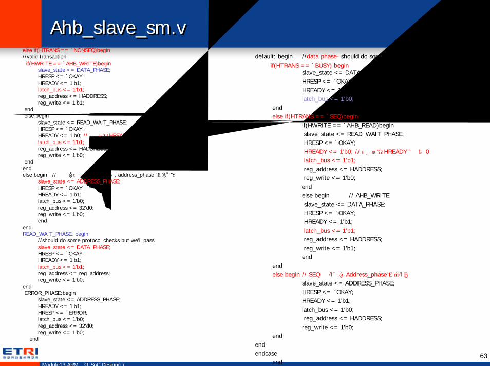
63Module13 ARM기반 SoC Design(I)
Ahb_slave_sm.vAhb_slave_sm.velse if(HTRANS == `NONSEQ)begin//valid transaction
if(HWRITE == `AHB_WRITE)beginslave_state <= DATA_PHASE;HRESP <= `OKAY;HREADY <= 1'b1;latch_bus <= 1'b1;reg_address <= HADDRESS;reg_write <= 1'b1;
endelse begin
slave_state <= READ_WAIT_PHASE;HRESP <= `OKAY;HREADY <= 1'b0; // 여기서만 HREADY 신호가 0 임latch_bus <= 1'b1;reg_address <= HADDRESS;reg_write <= 1'b0;
endendelse begin // 위의 모든 조건을 배제된면 , address_phase 로 머무름
slave_state <= ADDRESS_PHASE;HRESP <= `OKAY;HREADY <= 1'b1;latch_bus <= 1'b0;reg_address <= 32'd0;reg_write <= 1'b0; end
endREAD_WAIT_PHASE: begin
//should do some protocol checks but we'll passslave_state <= DATA_PHASE;HRESP <= `OKAY;HREADY <= 1'b1;latch_bus <= 1'b1;reg_address <= reg_address;reg_write <= 1'b0;
endERROR_PHASE:begin
slave_state <= ADDRESS_PHASE;HREADY <= 1'b1;HRESP <= `ERROR;latch_bus <= 1'b0;reg_address <= 32'd0;reg_write <= 1'b0;
end
default: begin //data phase- should do some protocol checks but we'll passif(HTRANS == `BUSY) begin
slave_state <= DATA_PHASE;HRESP <= `OKAY;HREADY <= 1'b1;latch_bus <= 1'b0;
endelse if(HTRANS == `SEQ)begin
if(HWRITE == `AHB_READ)beginslave_state <= READ_WAIT_PHASE;HRESP <= `OKAY;HREADY <= 1'b0; // 여기서만 HREADY 신호가 0 임latch_bus <= 1'b1;reg_address <= HADDRESS;reg_write <= 1'b0;
endelse begin // AHB_WRITE slave_state <= DATA_PHASE; HRESP <= `OKAY;HREADY <= 1'b1;latch_bus <= 1'b1;reg_address <= HADDRESS;reg_write <= 1'b1;
endendelse begin // SEQ 이 아니면 Address_phase로 돌아감
slave_state <= ADDRESS_PHASE;HRESP <= `OKAY;HREADY <= 1'b1;latch_bus <= 1'b0;reg_address <= HADDRESS;
reg_write <= 1'b0; end
endendcase
end
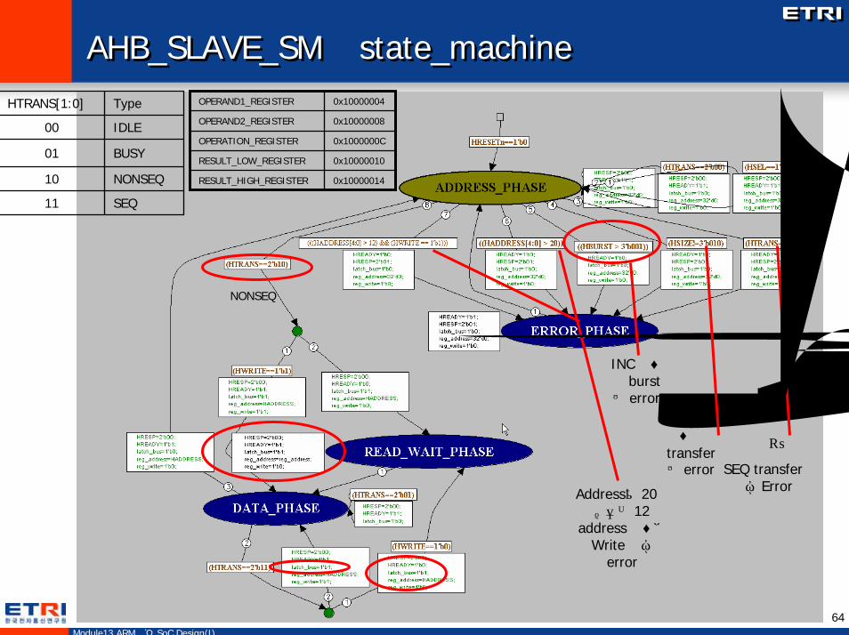
64Module13 ARM기반 SoC Design(I)
AHB_SLAVE_SM의 state_machineAHB_SLAVE_SM의 state_machineHTRANS[1:0] Type
00 IDLE
01 BUSY
10 NONSEQ
11 SEQ
Address가 20을넘거나 12
address 이상에Write 하면
error
OPERAND1_REGISTER 0x10000004
OPERAND2_REGISTER 0x10000008
OPERATION_REGISTER 0x1000000C
RESULT_LOW_REGISTER 0x10000010
RESULT_HIGH_REGISTER 0x10000014
32bit 이상의
transfer 는 error
처음부터
SEQ transfer이면 Error
INC 이상의 burst 는 error
NONSEQ
65Module13 ARM기반 SoC Design(I)
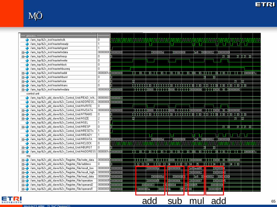
결과 파형결과 파형
add sub mul add
66Module13 ARM기반 SoC Design(I)
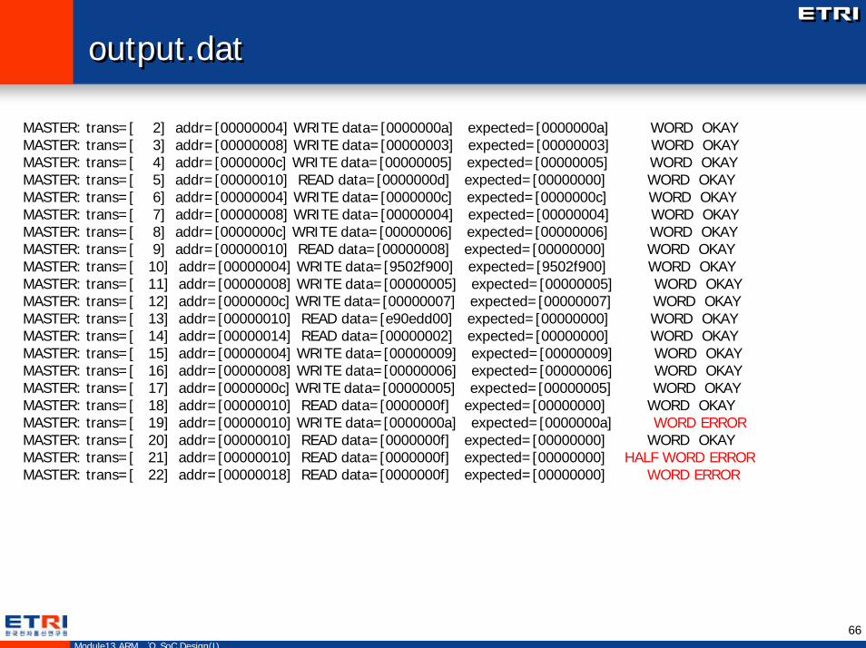
output.datoutput.dat
MASTER: trans=[ 2] addr=[00000004] WRITE data=[0000000a] expected=[0000000a] WORD OKAYMASTER: trans=[ 3] addr=[00000008] WRITE data=[00000003] expected=[00000003] WORD OKAYMASTER: trans=[ 4] addr=[0000000c] WRITE data=[00000005] expected=[00000005] WORD OKAYMASTER: trans=[ 5] addr=[00000010] READ data=[0000000d] expected=[00000000] WORD OKAYMASTER: trans=[ 6] addr=[00000004] WRITE data=[0000000c] expected=[0000000c] WORD OKAYMASTER: trans=[ 7] addr=[00000008] WRITE data=[00000004] expected=[00000004] WORD OKAYMASTER: trans=[ 8] addr=[0000000c] WRITE data=[00000006] expected=[00000006] WORD OKAYMASTER: trans=[ 9] addr=[00000010] READ data=[00000008] expected=[00000000] WORD OKAYMASTER: trans=[ 10] addr=[00000004] WRITE data=[9502f900] expected=[9502f900] WORD OKAYMASTER: trans=[ 11] addr=[00000008] WRITE data=[00000005] expected=[00000005] WORD OKAYMASTER: trans=[ 12] addr=[0000000c] WRITE data=[00000007] expected=[00000007] WORD OKAYMASTER: trans=[ 13] addr=[00000010] READ data=[e90edd00] expected=[00000000] WORD OKAYMASTER: trans=[ 14] addr=[00000014] READ data=[00000002] expected=[00000000] WORD OKAYMASTER: trans=[ 15] addr=[00000004] WRITE data=[00000009] expected=[00000009] WORD OKAYMASTER: trans=[ 16] addr=[00000008] WRITE data=[00000006] expected=[00000006] WORD OKAYMASTER: trans=[ 17] addr=[0000000c] WRITE data=[00000005] expected=[00000005] WORD OKAYMASTER: trans=[ 18] addr=[00000010] READ data=[0000000f] expected=[00000000] WORD OKAYMASTER: trans=[ 19] addr=[00000010] WRITE data=[0000000a] expected=[0000000a] WORD ERRORMASTER: trans=[ 20] addr=[00000010] READ data=[0000000f] expected=[00000000] WORD OKAYMASTER: trans=[ 21] addr=[00000010] READ data=[0000000f] expected=[00000000] HALF WORD ERRORMASTER: trans=[ 22] addr=[00000018] READ data=[0000000f] expected=[00000000] WORD ERROR
67Module13 ARM기반 SoC Design(I)
Altera_mf.v(C:₩quartus₩eda₩sim_lib)Altera_mf.v(C:₩quartus₩eda₩sim_lib)
68Module13 ARM기반 SoC Design(I)
QuizQuiz
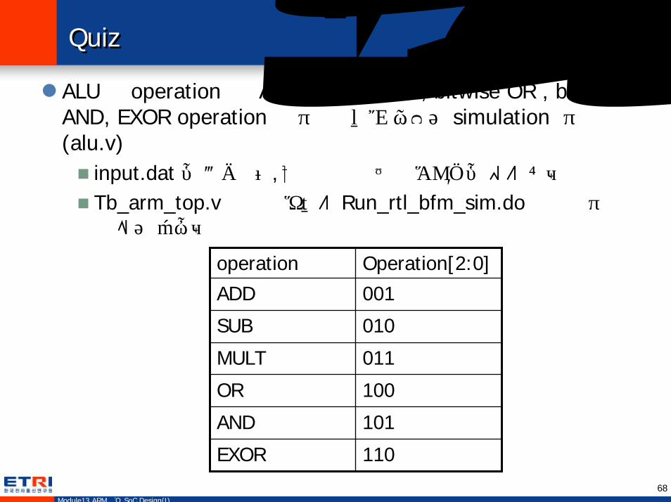
ALU 의 operation 을 ADD, SUB, MULT, bitwise OR , bitwise AND, EXOR operation 을 수행하도록 바꾸고 simulation 수행(alu.v)
input.dat 를 변경하여, 본인이 원하는 출력결과를 얻어 볼것Tb_arm_top.v 파일을 만들어 Run_rtl_bfm_sim.do 파일을 수행하지 않고 돌릴것
operation Operation[2:0]ADD 001
SUB 010
MULT 011
OR 100
AND 101
EXOR 110
69Module13 ARM기반 SoC Design(I)
ReferenceReference
Excalibur Devices Hardware Reference Manual, Altera CorporationExcalibur Bus Functional Model User Guide, Altera
CorporationModelsim command reference manual, Mentor
Graphics