1.introduction and application. 2.dopant solid solubility and sheet resistance. 3.microscopic view...
TRANSCRIPT
1
1. Introduction and application.
2. Dopant solid solubility and sheet resistance.
3. Microscopic view point: diffusion equations.
4. Physical basis for diffusion.
5. Non-ideal and extrinsic diffusion.
6. Dopant segregation and effect of oxidation.
7. Manufacturing and measurement methods.
Chapter 7 Dopant Diffusion
NE 343: Microfabrication and thin film technologyInstructor: Bo Cui, ECE, University of Waterloo; http://ece.uwaterloo.ca/~bcui/Textbook: Silicon VLSI Technology by Plummer, Deal and Griffin
2
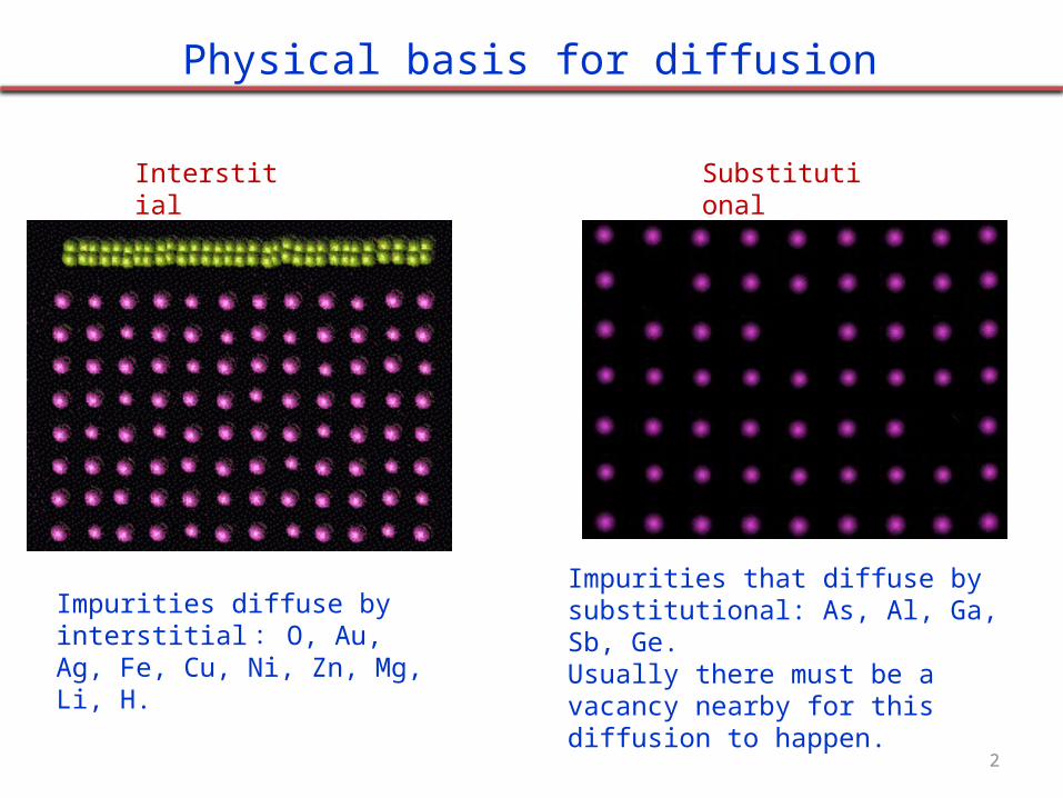
Interstitial Substitutional
Impurities diffuse by interstitial: O, Au, Ag, Fe, Cu, Ni, Zn, Mg, Li, H.
Impurities that diffuse by substitutional: As, Al, Ga, Sb, Ge.Usually there must be a vacancy nearby for this diffusion to happen.
Physical basis for diffusion
3
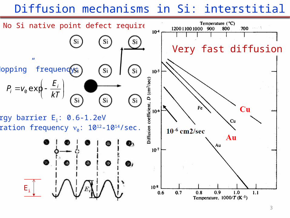
Diffusion mechanisms in Si: interstitialNo Si native point defect required
Very fast diffusion
“Hopping” frequency:
kT
EvP i
i exp0
Energy barrier Ei: 0.6-1.2eVVibration frequency 0: 1012-1014/sec.
Ei
4
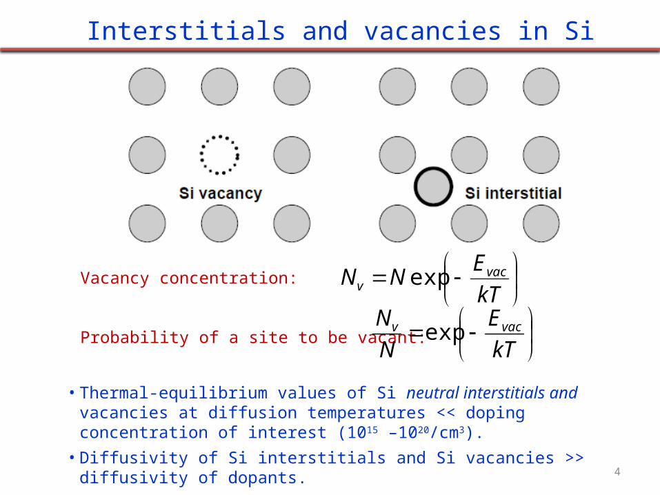
• Thermal-equilibrium values of Si neutral interstitials and vacancies at diffusion temperatures << doping concentration of interest (1015 –1020/cm3).• Diffusivity of Si interstitials and Si vacancies >> diffusivity of dopants.
Interstitials and vacancies in Si
kT
ENN vac
v expVacancy concentration:
Probability of a site to be vacant:
kT
E
N
N vacv exp
5
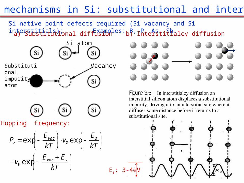
Si native point defects required (Si vacancy and Si interstitials); Examples: B, P, As, Sb.
Diffusion mechanisms in Si: substitutional and interstitialcy
b) Interstitialcy diffusiona) Substitutional diffusion
Si atom
VacancySubstitutional impurity atom
“Hopping” frequency:
kT
EEv
kT
Ev
kT
EP
svac
svacv
exp
expexp
0
0
Es: 3-4eV
6
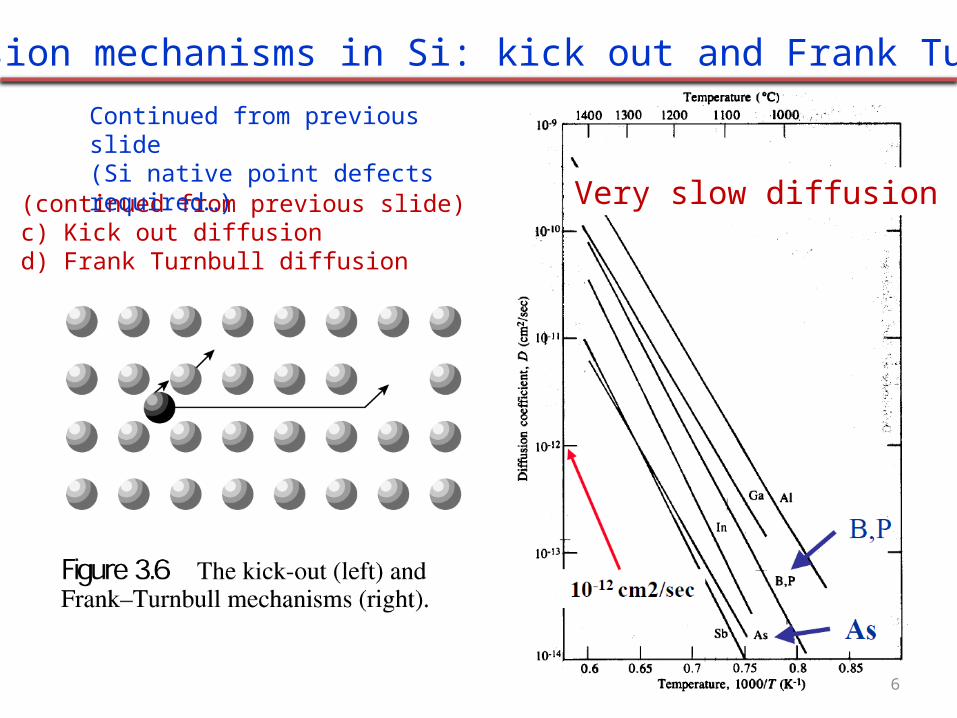
Diffusion mechanisms in Si: kick out and Frank Turnbull
(continued from previous slide)c) Kick out diffusiond) Frank Turnbull diffusion
Continued from previous slide(Si native point defects required…)
Very slow diffusion
7
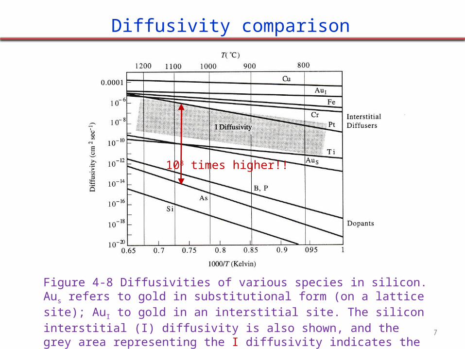
Diffusivity comparison
108 times higher!!
Figure 4-8 Diffusivities of various species in silicon. Aus refers to gold in substitutional form (on a lattice site); AuI to gold in an interstitial site. The silicon interstitial (I) diffusivity is also shown, and the grey area representing the I diffusivity indicates the uncertainty in this parameter.
8
1. Introduction and application.
2. Dopant solid solubility and sheet resistance.
3. Microscopic view point: diffusion equations.
4. Physical basis for diffusion.
5. Non-ideal and extrinsic diffusion.
6. Dopant segregation and effect of oxidation.
7. Manufacturing and measurement methods.
Chapter 7 Dopant Diffusion
NE 343 Microfabrication and thin film technologyInstructor: Bo Cui, ECE, University of WaterlooTextbook: Silicon VLSI Technology by Plummer, Deal and Griffin
9
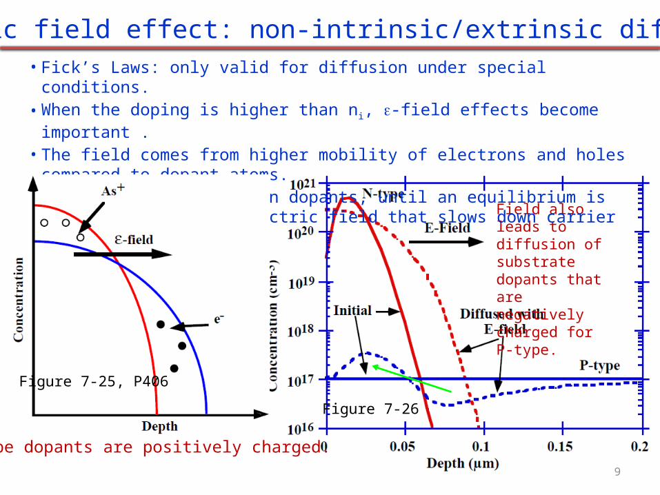
Field also leads to diffusion of substrate dopants that are negatively charged for P-type.
Electric field effect: non-intrinsic/extrinsic diffusion• Fick’s Laws: only valid for diffusion under special conditions.• When the doping is higher than ni, -field effects become important .• The field comes from higher mobility of electrons and holes compared to dopant atoms.• Carries move faster than dopants, until an equilibrium is attained due to the electric field
that slows down carrier and speeds up dopant.
N-type dopants are positively charged.
Figure 7-25, P406
Figure 7-26
10
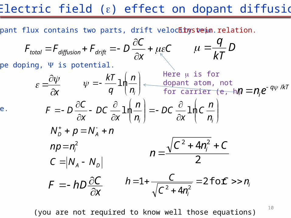
Cx
CDFFF driftdiffusiontotal
DkT
q
ii n
nC
xDC
n
n
xDC
x
CDF lnln
x
in
n
q
kTln
Electric field () effect on dopant diffusion
Total dopant flux contains two parts, drift velocity v=.
For n-type doping, is potential.
Therefore.
Einstein relation.
DA
i
AD
NNC
nnp
nNpN
2
24 22 CnC
n i
xChDF i
i
nCnC
Ch
for 24
122
(you are not required to know well those equations)
Here is for dopant atom, not for carrier (e, h)
kTqienn /
11
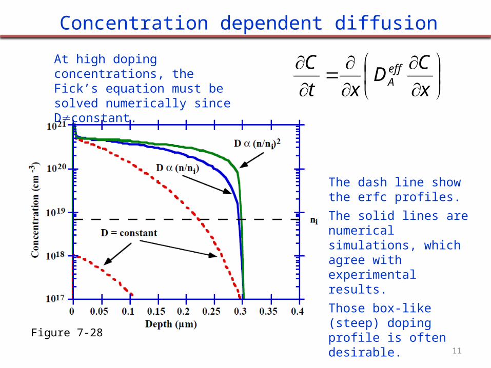
Concentration dependent diffusion
At high doping concentrations, the Fick’s equation must be solved numerically since Dconstant.
x
CD
xt
C effA
The dash line show the erfc profiles.
The solid lines are numerical simulations, which agree with experimental results.
Those box-like (steep) doping profile is often desirable.
Figure 7-28
12
1. Introduction and application.
2. Dopant solid solubility and sheet resistance.
3. Microscopic view point: diffusion equations.
4. Physical basis for diffusion.
5. Non-ideal and extrinsic diffusion.
6. Dopant segregation and effect of oxidation.
7. Manufacturing and measurement methods.
Chapter 7 Dopant Diffusion
NE 343 Microfabrication and thin film technologyInstructor: Bo Cui, ECE, University of WaterlooTextbook: Silicon VLSI Technology by Plummer, Deal and Griffin
13
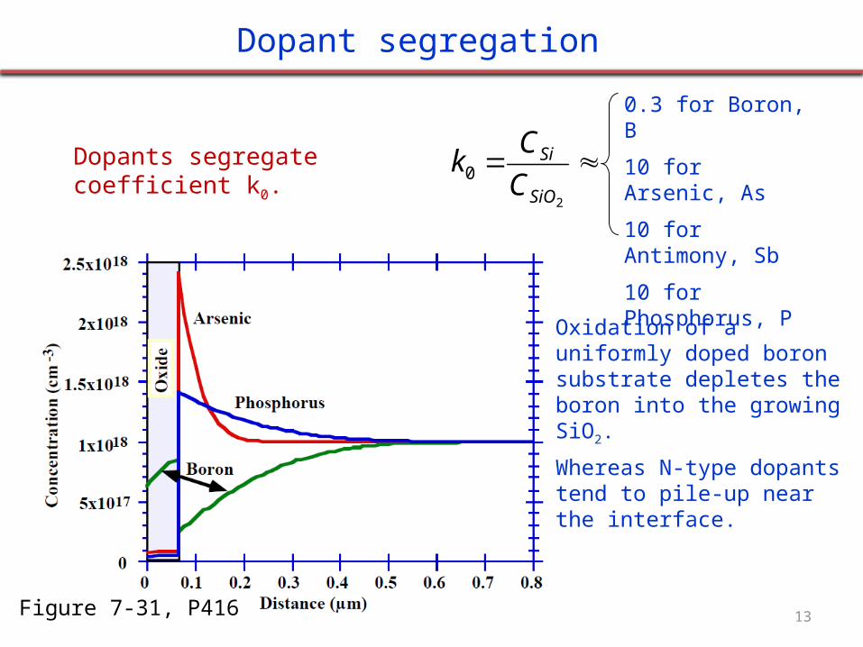
Dopant segregation
Dopants segregate coefficient k0. 2
0SiO
Si
C
Ck
0.3 for Boron, B
10 for Arsenic, As
10 for Antimony, Sb
10 for Phosphorus, P
Oxidation of a uniformly doped boron substrate depletes the boron into the growing SiO2.
Whereas N-type dopants tend to pile-up near the interface.
Figure 7-31, P416

14
Interfacial dopant pile-up during oxidation
Dopants may also segregate to an interface layer, perhaps only a monolayer thick.
They are not active (do not contribute electrons/holes).
This may consume up to 50% of the dose in a shallow layer.
Figure 7-32
15
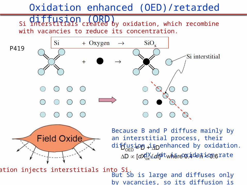
Oxidation enhanced (OED)/retarded diffusion (ORD)
Si interstitials created by oxidation, which recombine with vacancies to reduce its concentration.
Oxidation injects interstitials into Si.
Because B and P diffuse mainly by an interstitial process, their diffusion is enhanced by oxidation.
dXox/dt is oxidation rate
But Sb is large and diffuses only by vacancies, so its diffusion is suppressed/retarded.
P419
16
1. Introduction and application.
2. Dopant solid solubility and sheet resistance.
3. Microscopic view point: diffusion equations.
4. Physical basis for diffusion.
5. Non-ideal and extrinsic diffusion.
6. Dopant segregation and effect of oxidation.
7. Manufacturing and measurement methods.
Chapter 7 Dopant Diffusion
NE 343 Microfabrication and thin film technologyInstructor: Bo Cui, ECE, University of WaterlooTextbook: Silicon VLSI Technology by Plummer, Deal and Griffin
17
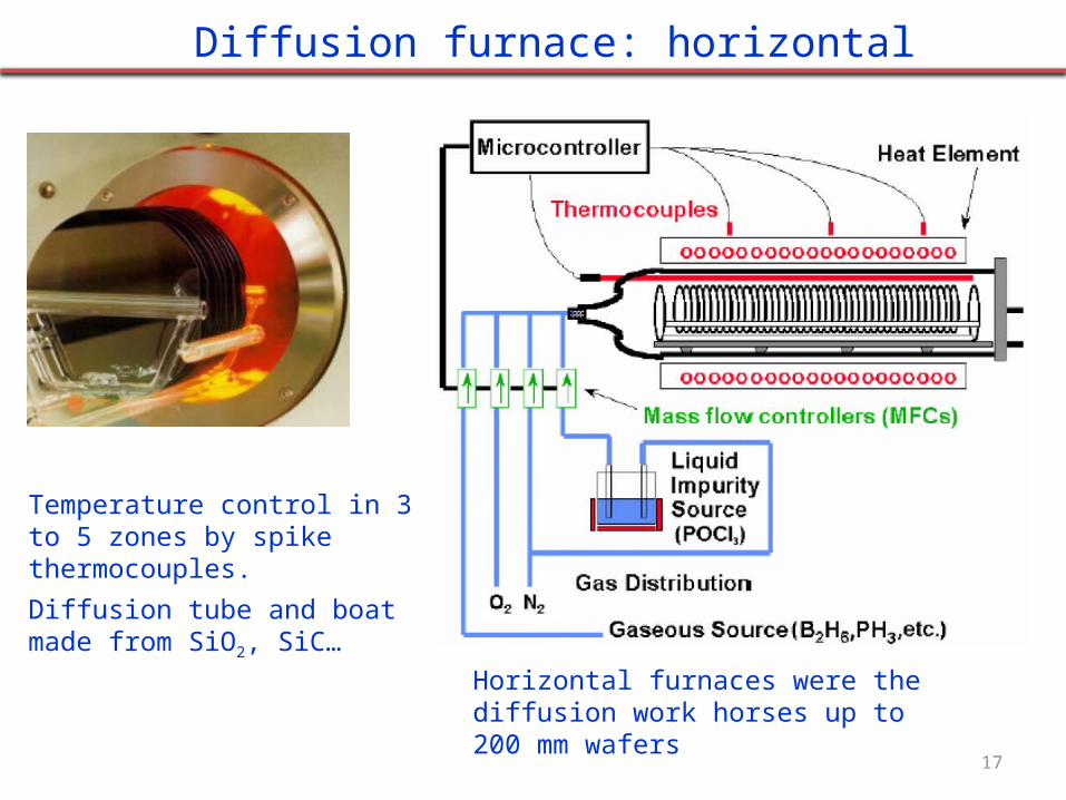
Diffusion furnace: horizontal
Temperature control in 3 to 5 zones by spike thermocouples.
Diffusion tube and boat made from SiO2, SiC…
Horizontal furnaces were the diffusion work horses up to 200 mm wafers
18
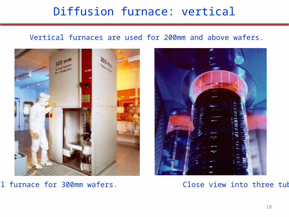
Vertical furnace for 300mm wafers. Close view into three tubes
Vertical furnaces are used for 200mm and above wafers.
Diffusion furnace: vertical
19
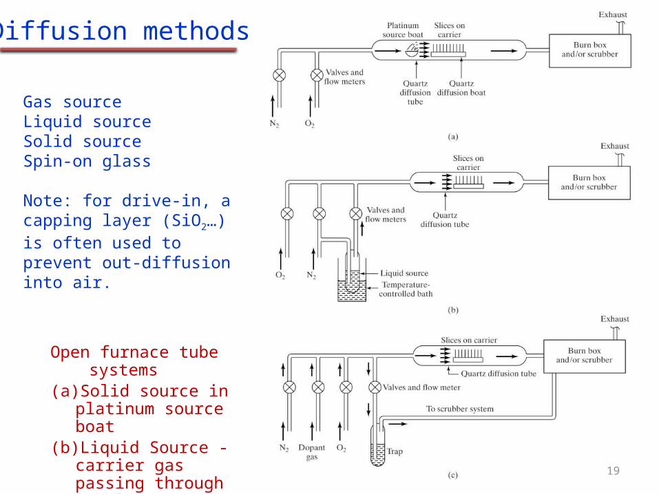
Open furnace tube systems(a) Solid source in platinum
source boat(b) Liquid Source - carrier gas
passing through bubbler(c) Gaseous impurity source
Gas sourceLiquid sourceSolid sourceSpin-on glass
Note: for drive-in, a capping layer (SiO2…) is often used to prevent out-diffusion into air.
Diffusion methods
20
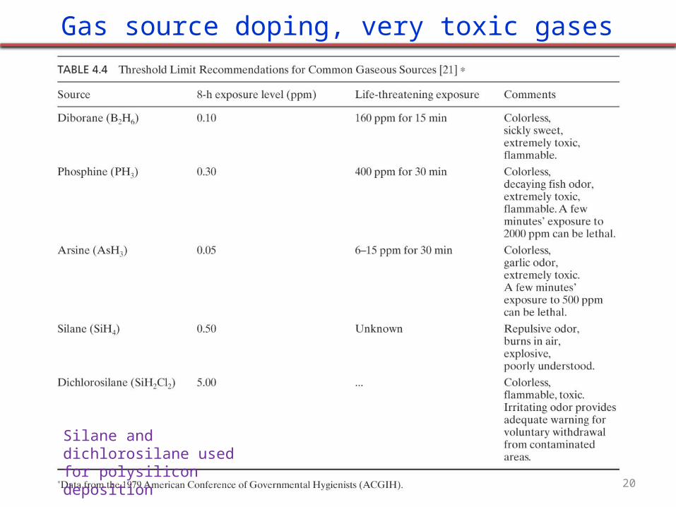
Gas source doping, very toxic gases
Silane and dichlorosilane used for polysilicon deposition
21
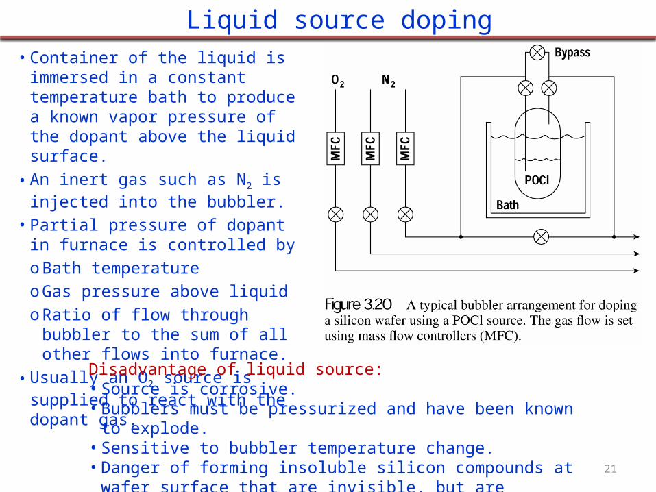
Liquid source doping• Container of the liquid is immersed in a
constant temperature bath to produce a known vapor pressure of the dopant above the liquid surface.• An inert gas such as N2 is injected into
the bubbler.• Partial pressure of dopant in furnace is
controlled byoBath temperatureoGas pressure above liquidoRatio of flow through bubbler to the
sum of all other flows into furnace.• Usually an O2 source is supplied to react
with the dopant gas.
Disadvantage of liquid source:• Source is corrosive.• Bubblers must be pressurized and have been known to explode.• Sensitive to bubbler temperature change.• Danger of forming insoluble silicon compounds at wafer surface that are
invisible, but are extremely undesirable.

22
Solid source doping
Another way is to use discs that are side-by-side to the Si wafer.For example, for diffusing p-type layers in Si, boron nitride (BN) disc is used. When oxidized at 750-1100 , a thin film of B℃ 2O3 forms at the surface.
In presence of H2, the volatile compound HBO2 forms and diffuses to wafer surface where a borosilicate glass in formed.This glass serves as the boron source for diffusion into the substrate.
No carrier gas needed, but protected under N2 or Ar gas.
23
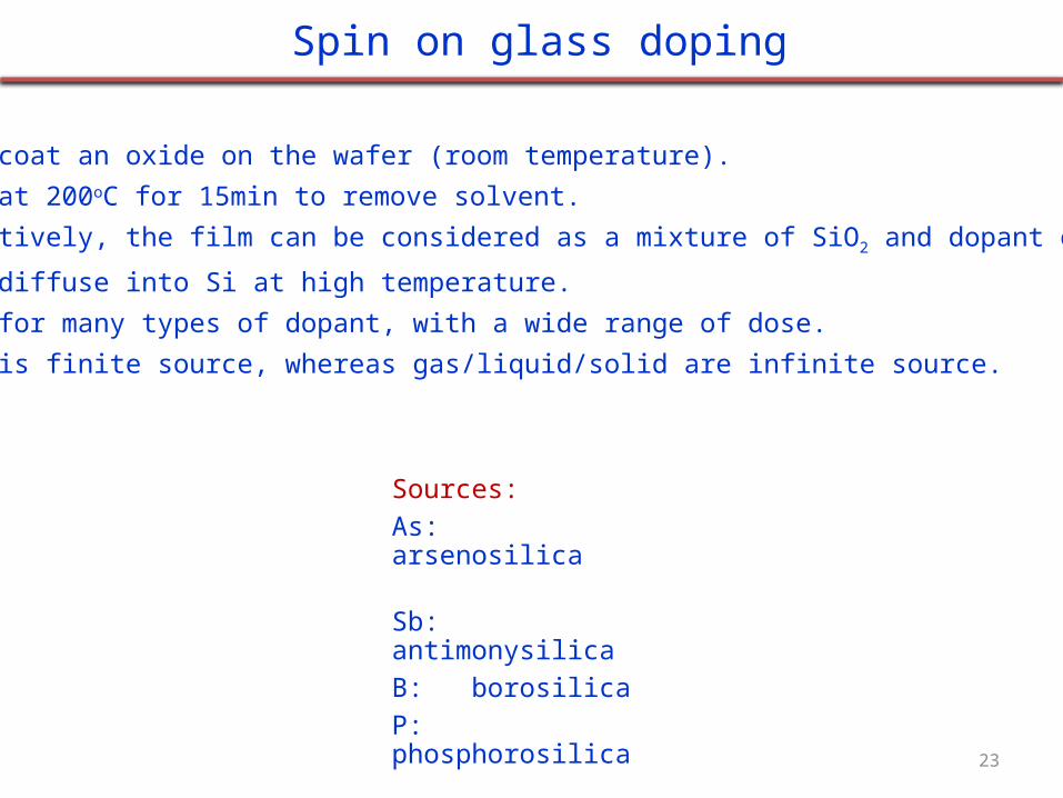
Spin on glass doping
• Spin-coat an oxide on the wafer (room temperature).• Bake at 200oC for 15min to remove solvent.
• Effectively, the film can be considered as a mixture of SiO2 and dopant oxide.
• Then diffuse into Si at high temperature.• Good for many types of dopant, with a wide range of dose.• This is finite source, whereas gas/liquid/solid are infinite source.
Sources:As: arsenosilica Sb: antimonysilicaB: borosilicaP: phosphorosilica
OHCOOBCOHB
OHOBOHBC
C
o
o
232300
262
232300
262
366
33
232 3432 SiOBSiOB
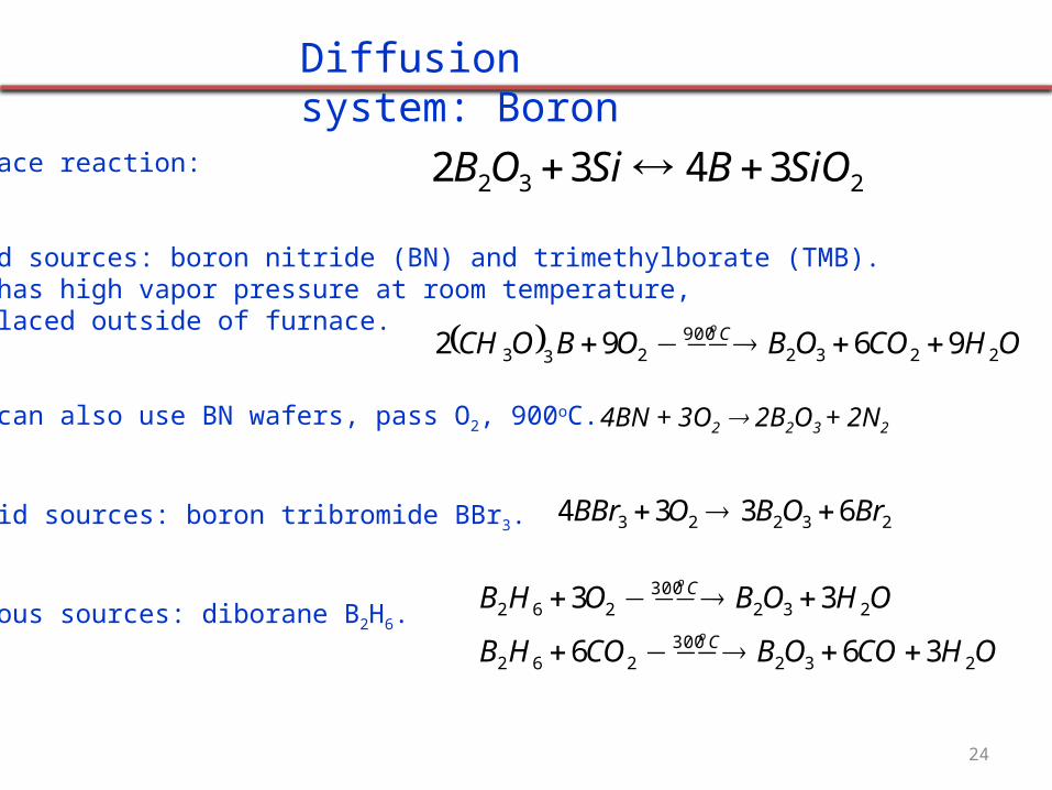
Diffusion system: Boron
Surface reaction:
Solid sources: boron nitride (BN) and trimethylborate (TMB).TMB has high vapor pressure at room temperature,so placed outside of furnace.
One can also use BN wafers, pass O2, 900oC.
Liquid sources: boron tribromide BBr3.
Gaseous sources: diborane B2H6.
OHCOOBOBOCH Co
2232900
233 9692
23223 6334 BrOBOBBr
4BN + 3O2 2B2O3 + 2N2
24
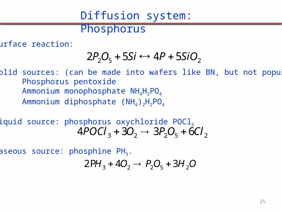
OHOPOH 25223 342P
252 5452 SiOPSiOP
Diffusion system: Phosphorus
Surface reaction:
Solid sources: (can be made into wafers like BN, but not popular) Phosphorus pentoxide Ammonium monophosphate NH4H2PO4
Ammonium diphosphate (NH4)2H2PO4
Liquid source: phosphorus oxychloride POCl3
Gaseous source: phosphine PH3.
25223 6334 ClOPOPOCl
25
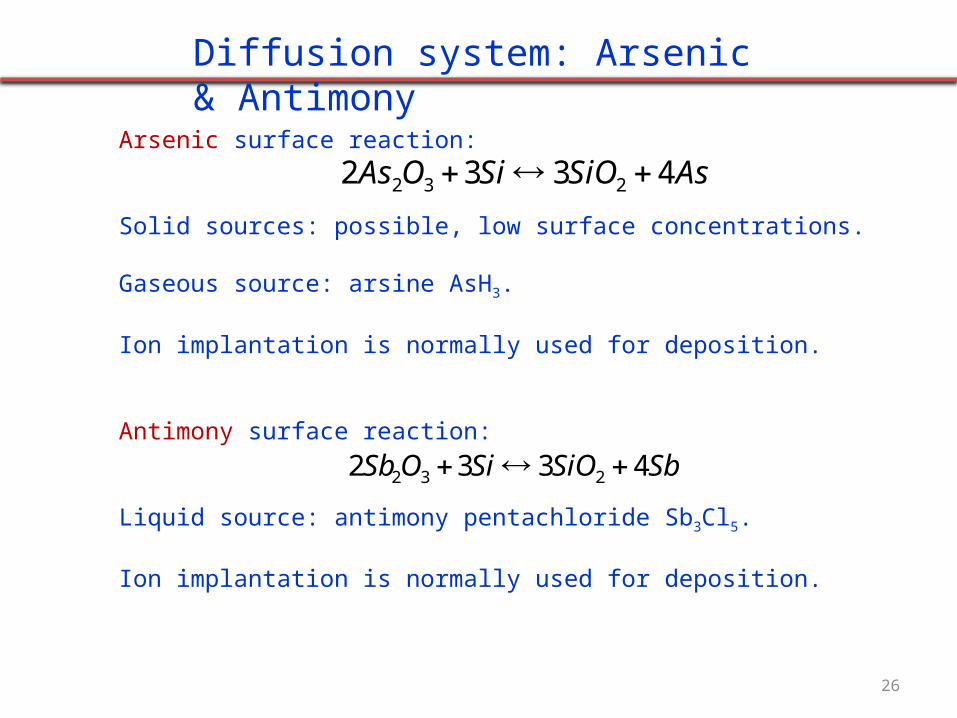
Diffusion system: Arsenic & Antimony
AsSiOSiOAs 4332 232
SbSiOSiOSb 4332 232
Arsenic surface reaction:
Solid sources: possible, low surface concentrations.
Gaseous source: arsine AsH3.
Ion implantation is normally used for deposition.
Antimony surface reaction:
Liquid source: antimony pentachloride Sb3Cl5.
Ion implantation is normally used for deposition.
26
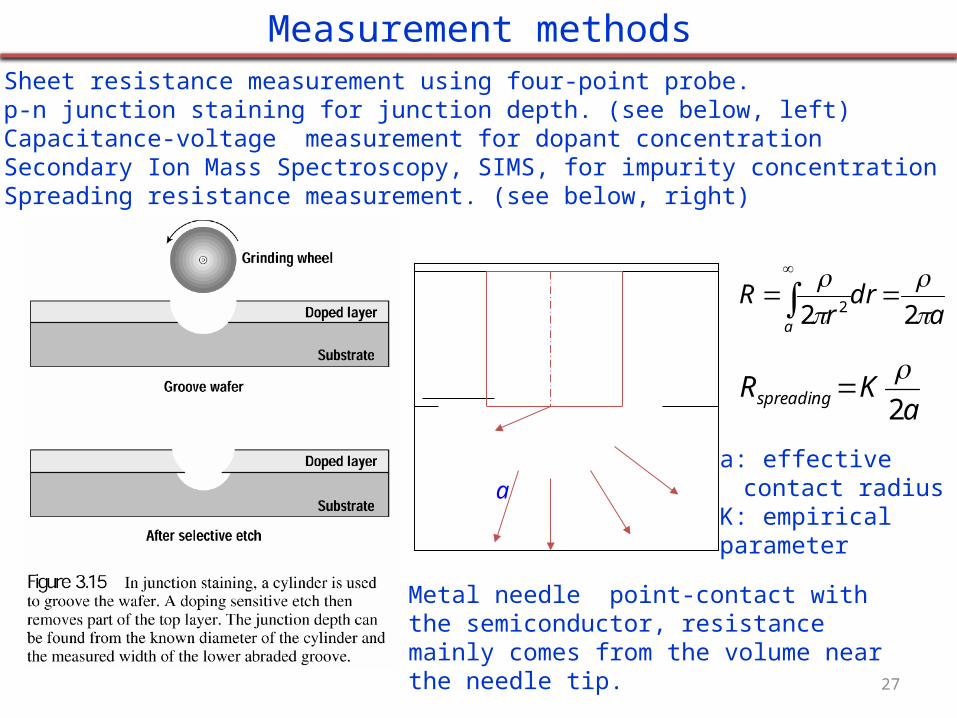
27
Measurement methods• Sheet resistance measurement using four-point probe.• p-n junction staining for junction depth. (see below, left)• Capacitance-voltage measurement for dopant concentration• Secondary Ion Mass Spectroscopy, SIMS, for impurity concentration• Spreading resistance measurement. (see below, right)
a
adr
rR
a
22 2
aKRspreading 2
Metal needle point-contact with the semiconductor, resistance mainly comes from the volume near the needle tip.
a: effective contact radius
K: empirical parameter
28
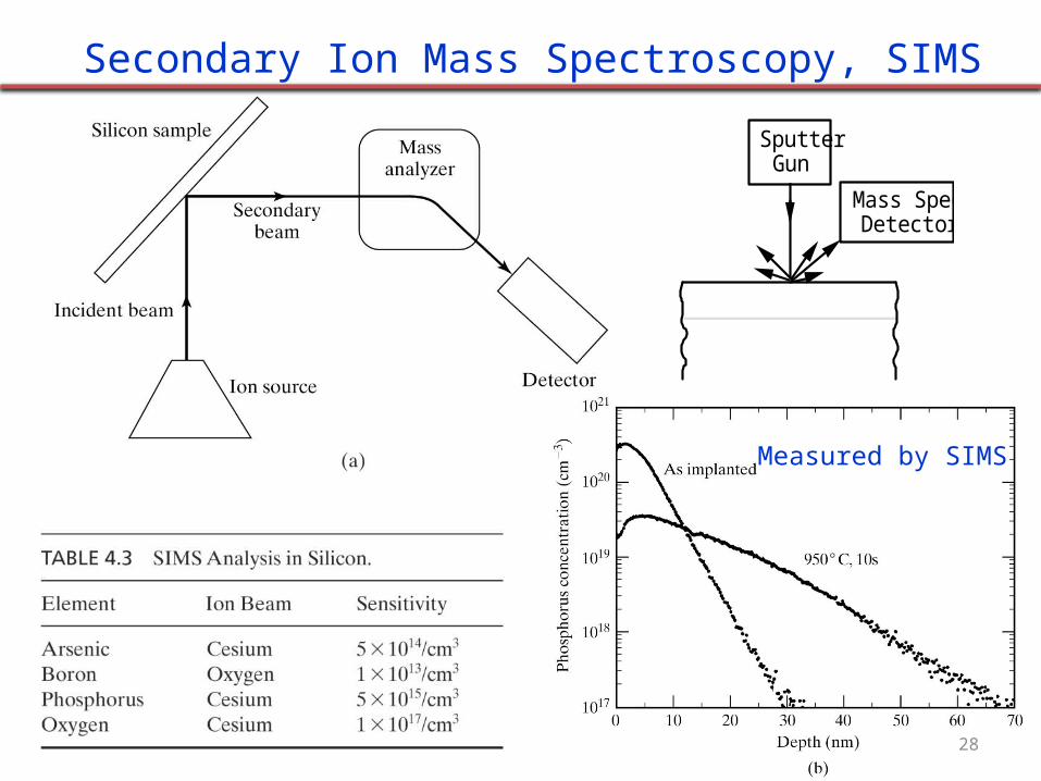
Mass Spec Detector
Sputter Gun
Secondary Ion Mass Spectroscopy, SIMS
Measured by SIMS