13.2 physical characteristics of a hard drivefaculty.etsu.edu/tarnoff/ntes2150/ch13_v02.pdf · in a...
TRANSCRIPT

269
CHAPTER THIRTEEN
Memory Hierarchy
13.1 Characteristics of the Memory Hierarchy We've discussed the organization and operation of RAM, but RAM
is only one level of the group of components used to store information in a computer. The hard drive, for example, stores all of the data and code for the computer in a non-volatile format, and unless a file has been opened, this information can only be found on the hard drive.
Even though the hard drive stores all of the data necessary to operate the computer, other storage methods are needed. This is for a number of reasons, most notably the hard drive is slow and running programs from it would be impossible. When the processor needs data or applications, it first loads them into main memory (RAM).
Main memory and the hard drive are two levels of the computer's memory hierarchy. A memory hierarchy is an organization of storage devices that takes advantage of the characteristics of different storage technologies in order to improve the overall performance of a computer system. Figure 13-1 presents the components of the standard memory hierarchy of a computer. Each of these components and their function in the hierarchy is described in this chapter.
Figure 13-1 Block Diagram of a Standard Memory Hierarchy
13.2 Physical Characteristics of a Hard Drive At the bottom of the hierarchy is long-term, high-capacity storage.
This type of storage is slow making a poor choice for the processor to use for execution of programs and data access. It is, however, necessary to provide computer systems with high capacity, non-volatile storage.
registers cache RAM(s) main memory
long term storage, e.g., hard drive
Increasing capacity
Increasingspeed

270 Computer Organization and Design Fundamentals
Hard drives are the most cost-effective method of storing data. In the mid-1980's, a 30 Megabyte hard drive could be purchased for around $300 or about $10 per MB. In 2007, retailers advertised a 320 Gigabyte SATA Hard drive for around $80 or about $0.00025 per MB. In other words, the cost to store a byte of data is almost 1/40,000th cheaper today than it was a little over two decades ago.
Hard drives store data in well-organized patterns of ones and zeros across a thin sheet of magnetic material. This magnetic material is spread either on one or both sides of a lightweight, rigid disk called a substrate. The substrate needs to be lightweight because it is meant to spin at very high speeds. The combination of magnetic material and substrate is called a platter.
The more rigid the substrate is, the better the reliability of the disk. This was especially true when the mechanisms that were used to read and write data from and to the disks were fixed making them prone to scraping across the substrate's surface if the substrate was not perfectly flat. The condition where the read-write mechanism comes in contact with the disk is called a "crash" which results in magnetic material being scraped away from the disk.
Substrates used to be made from aluminum. Unfortunately, extreme heat sometimes warped the aluminum disk. Now glass is used as a substrate. It improves on aluminum by adding:
• better surface uniformity which increases reliability; • fewer surface defects which reduces read/write errors; • better resistance to warping; • better resistance to shock; and • the ability to have the read/write mechanism ride closer to the
surface allowing for better data density.
13.2.1 Hard Drive Read/Write Head Data is recorded to the platter using a conductive coil called a head.
Older drives and floppy drives use the same head for reading the data too. The head is shaped like a "C" with the gap between the ends positioned to face the magnetic material. A coil of wire is wrapped around the portion of the head that is furthest from the magnetic material. Figure 13-2 shows the configuration of this type of head.
In order to write data, an electrical current is passed through the wire creating a magnetic field within the gap of the head close to the disk.

Chapter 13: Memory Hierarchy 271
This field magnetizes the material on the platter in a specific direction. Reversing the current would polarize the magnetic material in the opposite direction. By spinning the platter under the head, patterns of magnetic polarization can be stored in circular paths on the disk. By moving the head along the radius, nested circular paths can be created. The magnetized patterns on the platter represent the data.
Figure 13-2 Configuration of a Hard Drive Write Head
It is possible to use the same head to read data back from the disk. If a magnetized material moves past a coil of wire, it produces a small current. This is the same principle that allows the alternator in your car to produce electricity. The direction of the current generated by the disk's motion changes if the direction of the magnetization changes. In this way, the same coil that is used to write the data can be used to read it. Just like the alternator in your car though, if the disk is not spinning, no current is generated that can be used to read the data.
Newer hard drives use two heads, one for reading and one for writing. The newer read heads are made of a material that changes its resistance depending on the magnetic field that is passing under it. These changes in resistance affect a current that the hard drive controller is passing through the read head during the read operation. In this way, the hard drive controller can detect changes in the magnetic polarization of the material directly under the read head.
There is another characteristic of the read/write head that is important to the physical operation of the hard drive. As was stated earlier, the area that is polarized by the head is equal to the gap in the write head. To polarize a smaller area thereby increasing the data density, the gap must be made smaller. To do this, the distance between the head and the platter must be reduced. Current technology allows heads to "fly" at less then three micro inches above the platter surface.
Direction of rotation
Magnetic coating
Substrate
Write head
Write current

272 Computer Organization and Design Fundamentals
When the magnetic material is deposited on a flexible substrate such as a floppy diskette or a cassette tape, the flex in the material makes it possible for the head to come in contact with the substrate without experiencing reliability problems. This is not true for hard disks. Since the platters are rigid and because the platters spin at thousands of rotations per minute, any contact that the head makes with the platter will result in magnetic material being scraped off. In addition, the heat from the friction will eventually cause the head to fail.
These two issues indicate that the read/write head should come as close to the platters as possible without touching. Originally, this was done by making the platter as flat as possible while mounting the head to a rigid arm. The gap would hopefully stay constant. Any defects or warpage in the platter, however, would cause the head to crash onto the platter resulting in damaged data.
A third type of head, the Winchester head or "flying head" is designed to float on a cushion of air that keeps it a fixed distance from the spinning platter. This is done by shaping the head into an airfoil that takes advantage of the air current generated by the spinning platter. This means that the head can operate much closer to the surface of the platter and avoid crashing even if there are imperfections.
13.2.2 Data Encoding It might seem natural to use the two directions of magnetic
polarization to represent ones and zeros. This is not the case, however. One reason for this is that the controllers detect the changes in magnetic direction, not the direction of the field itself. Second, large blocks of data that are all ones or all zeros would be difficult to read because eventually the controller might lose track or synchronization of where one bit ended and the next began.
The typical method for storing data to a platter involves setting up a clock to define the bit positions, and watching how the magnetic field changes with respect to that clock. Each period of the clock defines a single bit time, e.g., if a single bit takes 10 nanoseconds to pass under the read-write head when the platter is spinning, then a clock with a period of 10 nanoseconds, i.e., a frequency of (10×10-9)-1 = 100 MHz is used to tell the controller when the next bit position is coming.
Originally, a magnetic field change at the beginning and middle of a bit time represented a logic one while a magnetic field change only at the beginning represented a logic zero. This method was referred to as Frequency Modulation (FM). Figure 13-3 uses an example to show the

Chapter 13: Memory Hierarchy 273
relationship between the bit-periods, the magnetic field changes, and the data stored using FM encoding.
Figure 13-3 Sample FM Magnetic Encoding
To store a one using FM encoding, the polarization of the magnetic field must change twice within the space of a bit. This means that in order to store a single bit, FM encoding takes twice the width of the smallest magnetic field that can be written to the substrate. If the maximum number of polarity changes per bit could be reduced, more data could be stored to the same disk.
Modified Frequency Modulation (MFM) does this by changing the way in which the magnetic polarization represents a one or a zero. MFM defines a change in polarization in the middle of a bit time as a one and no change in the middle as a zero. If two or more zeros are placed next to each other, a change in polarization is made between each of the bit times. This is done to prevent a stream zeros from creating a long block of unidirectional polarization. Figure 13-4 uses an example to show the relationship between the bit-periods, the magnetic field changes, and the data stored using MFM encoding.
For MFM encoding, the longest period between polarity changes occurs for the bit sequence 1-0-1. In this case, the polarity changes are separated by two bit periods. The shortest period between polarity changes occurs when a one follows a one or a zero follows a zero. In these cases, the polarity changes are separated by a single bit period. This allows us to double the data density over FM encoding using the same magnetic surface and head configuration. The hard drive controller, however, must be able to handle the increased data rate.
Run Length Limited (RLL) encoding uses polarity changes to define sequences of bits rather than single bits. By equating different patterns of polarity changes to different sequences of ones and zeros, the density of bits stored to a platter can be further increased. There is a
Polarity
Reversals
Value 1 0 0 1 0 1 1 1 0
single bit time

274 Computer Organization and Design Fundamentals
science behind generating these sequences and their corresponding polarity changes. It is based on satisfying the following requirements:
• to ensure enough polarity changes to maintain bit synchronization; • to ensure enough bit sequences are defined so that any sequence of
ones and zeros can be handled; and • to allow for the highest number of bits to be represented with the
fewest number of polarity changes.
Figure 13-4 Sample MFM Magnetic Encoding
Figure 13-5 presents a sample set of RLL encoding polarity changes and the bit sequences that correspond to each of them. Any pattern of ones and zeros can be represented using this sample set of sequences.
Figure 13-5 RLL Relation between Bit Patterns and Polarity Changes
Now the shortest period between polarity changes is one and a half bit periods producing a 50% increased density over MFM encoding. Figure 13-6 presents the same sample data with RLL encoding.
10
11
000
010
011
0010
0011
single bit time
Polarity
Reversals
Value
single bit time
1 0 0 1 0 1 1 1 0

Chapter 13: Memory Hierarchy 275
Figure 13-6 Sample RLL Magnetic Encoding
Improved encoding methods have been introduced since the development of RLL that use digital signal processing and other methods to realize better data densities. These methods include Partial Response, Maximum Likelihood (PRML) and Extended PRML (EPRML) encoding. A discussion of the details of these methods is beyond the scope of this text because it depends on a better understanding of sampling theory and electrical principles.
13.2.3 Hard Drive Access Time There are a number of issues affecting the latency between a device
requesting data and the hard drive responding with the data. Some of these issues depend on the current state of the system while others depend on the physical design of the drive and the amount of data being requested. There are four basic aspects to hard drive access time: queuing time, seek time, rotational latency, and transfer time.
After an initial request is made to a hard drive, the system must wait for the hard drive to become available. This is called queuing time. The hard drive may be busy serving another request or the bus or I/O channel that the hard drive uses may be busy serving another device that shares the link. In addition, the system's energy saving features may have powered down the drive meaning that an additional delay is incurred waiting for the drive to spin up.
The second aspect, seek time, is the amount of time it takes to get the read/write head from its current track to the desired track. Seek time is dependent on many things. First, it depends on the distance between the current and desired tracks. In addition, mechanical movement of any sort requires a ramping up before attaining maximum speed and a ramping down to avoid overshooting the desired target position. It is for these reasons that manufacturers publish a typical seek time.
Polarity
Reversals
Value 1 0 0 1 0 1 1 1 0
bit group bit group bit group bit group

276 Computer Organization and Design Fundamentals
Seek times have improved through the use of lighter components and better head positioning so that shorter seek distances are needed. As of this writing, the typical seek time for a hard drive is around 8 ms while higher performance drives might be as low as 4 ms. The heads used in CDROMs are heavier, and therefore, the seek time of a CDROM is longer than that of a hard drive. Older fixed head designs used multiple heads (one per track), each of which was stationary over its assigned track. In this case, the seek time was minimal, limited to the amount of time it took to electrically switch to the desired head.
Once the head has been positioned over the desired track, the drive must wait for the platters to rotate to the sector containing the requested data. This is called rotational latency. The worst case occurs when the start of the desired sector has just passed under the head when the drive begins looking for the data. This requires almost a full rotation of the platters before the drive can begin transferring the data. We can use the following calculation to determine the time required for a platter in a 7200 RPM drive to make a full rotation.
If we make the assumption that on average the desired sector will be
one half of a rotation away from the current position, then the average rotational latency should be half the time it takes for a full rotation. This means that for a 7200 RPM drive, the estimated rotational latency should be about 4.2 milliseconds.
Queuing time, seek time, and rotational latency are somewhat random in nature. Transfer time, however, is more predictable. Transfer time is the time it takes to send the requested data from the hard drive to the requesting device. Theoretically, the maximum transfer time equals the amount of time it takes for the data to pass beneath the head. If there are N sectors per track, then the amount of time it takes to retrieve a single sector can be calculated as shown below.
Theoretical transfer time for a sector = (N × rotational speed)-1
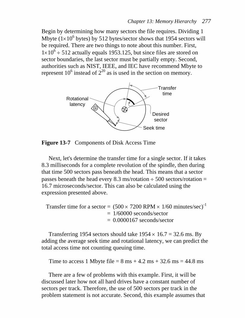
Figure 13-7 presents a graphical representation of seek time,
rotational latency, and transfer time. As an example, let's calculate the amount of time it would take to
read a 1 Mbyte file from a 7200 RPM drive with a typical 8 ms seek time that has 500 sectors per track each of which contains 512 bytes.
1 minute 7200 rotations
60 seconds1 minute × = 8.3 ms per rotation
Chapter 13: Memory Hierarchy 277
Begin by determining how many sectors the file requires. Dividing 1 Mbyte (1×106 bytes) by 512 bytes/sector shows that 1954 sectors will be required. There are two things to note about this number. First, 1×10⁶ ÷ 512 actually equals 1953.125, but since files are stored on sector boundaries, the last sector must be partially empty. Second, authorities such as NIST, IEEE, and IEC have recommend Mbyte to represent 106 instead of 220 as is used in the section on memory.
Figure 13-7 Components of Disk Access Time
Next, let's determine the transfer time for a single sector. If it takes 8.3 milliseconds for a complete revolution of the spindle, then during that time 500 sectors pass beneath the head. This means that a sector passes beneath the head every 8.3 ms/rotation ÷ 500 sectors/rotation = 16.7 microseconds/sector. This can also be calculated using the expression presented above.
Transfer time for a sector = (500 × 7200 RPM × 1/60 minutes/sec)-1 = 1/60000 seconds/sector = 0.0000167 seconds/sector
Transferring 1954 sectors should take 1954 × 16.7 = 32.6 ms. By
adding the average seek time and rotational latency, we can predict the total access time not counting queuing time.
Time to access 1 Mbyte file = 8 ms + 4.2 ms + 32.6 ms = 44.8 ms
There are a few of problems with this example. First, it will be
discussed later how not all hard drives have a constant number of sectors per track. Therefore, the use of 500 sectors per track in the problem statement is not accurate. Second, this example assumes that
Rotational latency
Seek time
Transfer time
Desired sector

278 Computer Organization and Design Fundamentals
the sectors of the file have been stored in consecutive locations. This is referred to as sequential access. Unfortunately sequential access is not always possible. File system fragmentation where the blocks of a file end up scattered across dissociated sectors of the hard disk hurts disk performance because each discontinuity in the order of the sectors forces the drive to incur an additional seek time and rotational latency.
Lastly, with 500 sectors per track, the almost 2000 sectors of this file will need to be stored on at least four tracks. Each time a drive is forced to switch tracks, an additional seek time and rotational latency will be incurred. In the case of our example, 12.2 ms must be added for each of the three additional tracks bringing the access time to 81.4 ms.
If the sectors of the file are stored randomly across the tracks of the platters, individual seek times and rotational latencies will be required for each sector. This is referred to as random access. In this case, each sector will take 8 ms + 4.2 ms + 0.017 ms = 12.217 ms to retrieve. Multiplying this by 1954 sectors means that retrieving the 1 Mbyte file in random access will take 23.872 seconds.
13.2.4 Self-Monitoring, Analysis & Reporting Technology System A hard drive crash rarely comes without a warning. The user may be
unaware of any changes in their hard drive's operation preceding a mechanical failure, but there are changes. For example, if a hard drive's platters are taking longer to get up to full speed, it may be that the bearings are going bad. A hard drive that has been experiencing higher than normal operating temperatures may also be about to fail.
Newer drives now support a feature referred to as Self-Monitoring Analysis and Reporting Technology (SMART). SMART enabled drives can provide an alert to the computer's BIOS warning of a parameter that is functioning outside of its normal range. This usually results in a message to the user to replace the drive before it fails.
SMART attribute values are stored in the hard drive as integers in the range from 1 to 253. Lower values indicate worse conditions. Depending on the parameter and the manufacturer, different failure thresholds are set for each of the parameters. The parameters measured vary from drive to drive with each drive typically monitoring about twenty. The following is a sample of some types of measurements:
• Power On Hours: This indicates the age of the drive. • Power Cycle Count: This also might be an indication of age.

Chapter 13: Memory Hierarchy 279
• Spin Up Time: A longer spin up time may indicate a problem with the assembly that spins the platters.
• Temperature: Higher temperatures also might indicate a problem with the assembly that spins the platters.
• Head Flying Height: A reduction in the flying height of a Winchester head may indicate it is about to crash into the platters.
There are still unpredictable failures such as the failure of an IC or a
failure caused by a catastrophic event such as a power surge, but now the user can be forewarned of most mechanical failures.
13.3 Organization of Data on a Hard Drive The width of a hard drive's read/write head is much smaller than that
of the platter. This means that there are a number of non-overlapping positions for the read/write head along the platter's radius. By allowing the movable read/write head to be positioned at intervals along the radius of the disk, information can be recorded to any of a number of concentric circles on the magnetic material. Each one of these circles is called a track. A typical hard drive disk contains thousands of tracks per inch (TPI) on a single side of a platter, each track being the width of the read/write head. Figure 13-8 shows how these tracks correspond to the movement and size of the read/write head.
Figure 13-8 Relation between Read/Write Head and Tracks
A small gap called an intertrack gap is placed between the tracks to avoid interference from neighboring data. Reducing this gap allows for more data to be stored on a disk, but it also increases the risk of having data corrupted when data from an adjacent track bleeds over.
Each track is divided into sections of around 512 bytes apiece. These sections are called sectors. A platter may have sectors that are
Head moves along disk's radius so it can be positioned over any of the concentric tracks.
The width of a track is equal to the width of the read/write head.
Direction of rotation

280 Computer Organization and Design Fundamentals
Intertrack gaps
Intersector gaps
Sectors
fixed in size for the whole platter or they may have variable amounts of data depending on their location on the platter relative to the center of rotation. There are typically hundreds of sectors per track.
In addition to the gaps left between the tracks, gaps are also left between the sectors. These gaps allow for a physical separation between the blocks of data and are typically used to help the hard drive controller when reading from or writing to the disk. These gaps are called intersector gaps. Figure 13-9 shows the relationship of these gaps to the tracks and sectors.
Figure 13-9 Organization of Hard Disk Platter
One way to increase the capacity of a hard drive is to increase the number of surfaces upon which the magnetic material is placed. The first way to do this is to place magnetic material on both sides of the platter. When this is done, a second read-write head must be placed on the opposite side of the platter to read the second magnetic surface. By using the same organization of sectors and tracks, this doubles the capacity of the hard drive.
A second method for increasing capacity is to mount multiple platters on a single spindle, the axis around which all of the platters rotate. Each additional magnetic surface adds to the capacity of the drive, and as with putting magnetic material on both sides of a single platter, all magnetic surfaces have the same organization of sectors and tracks, each sector lining up with the ones above it and below it. Every additional magnetic surface requires an additional read-write head.
All of the heads of a hard drive are locked together so that they are reading from the exact same location on each of their respective surfaces. Therefore, each track on each surface that is the same distance from the spindle can be treated as a unit because the hard drive controller is accessing them simultaneously. The set of all tracks, one

Chapter 13: Memory Hierarchy 281
from each surface, that are equidistant from the spindle are referred to as a cylinder. This virtual entity is depicted in Figure 13-10.
Figure 13-10 Illustration of a Hard Drive Cylinder
Using this information, we can develop a method for calculating the capacity of a hard drive. In general, the capacity of a hard drive equals the number of bytes per sector multiplied by the number of sectors per track multiplied by the number of cylinders multiplied by 2 if the platters have magnetic material on both sides and finally multiplied by the number of platters.
Figure 13-9 shows a platter that has the same number of sectors per track regardless of the radius of the track. From this figure, it can be seen that the physical size of a sector becomes smaller as its distance from the spindle is reduced. Since the number of bits per sector is constant, the size of a bit is also reduced.
Because the smallest allowable size for a bit is dictated by the size of the read-write head, the number of bits per track is limited by the number of bits that can fit on the smallest track, the one closest to the spindle. Because of this limitation, the outside tracks waste space when the bits become wider than is required by the head. Regardless of where the head is positioned, bits will pass under the head at a constant rate. This arrangement is called constant angular velocity (CAV).
A better use of the space on the platter can be realized by letting the width of all bits be defined by the width of the read-write head regardless of the track position. This allows for more bits to be stored on the outer tracks. This tighter arrangement of bits can be seen in the comparison of CAV Figure 13-11a with the equal sized bits in Figure 13-11b.
Platters
Tracks
Cylinder

282 Computer Organization and Design Fundamentals
Figure 13-11 Equal Number of Bits per Track versus Equal Sized Bits
The problem with doing this is that as the read-write head moves to the outer tracks, the rate at which the bits pass under the head increases dramatically over that for the smallest track. This contrasts with the fixed number of bits per track which has the same data rate regardless of the position of the read-write head. This means that the hard drive with the equal sized bits requires a more complex controller.
Regardless of how the bits are arranged on the platters, the number of bits per sector must remain constant for all tracks. Since partial sectors are not allowed, additional bits cannot be added to tracks further from the spindle until a full sector's worth of bits can be added. This creates "zones" where groups of neighboring tracks have the same number of sectors, and therefore, the same number of bits. This method is called Zone Bit Recording (ZBR). Figure 13-12 compares CAV with ZBR.
Figure 13-12 Comparison of Sector Organizations
a.) Equal number of bits b.) Equal sized bits
a.) Constant Angular Velocity b.) Zone Bit Recording

Chapter 13: Memory Hierarchy 283
This brings us to the next layer of data organization on a hard drive: formatting. Formatting is the process of setting or clearing bits on the platters in an effort to organize and locate the files that will be stored on the hard drive. The methods used by hard drives to organize data can also be found on other rotational storage media such as floppy disks and Zip® disks.
Every hard drive utilizes two types of formatting: low-level and O/S-level. Low-level formatting (LLF) depends on the mechanics of the hard drive and its controller. It divides the platters into usable subsections by defining the tracks and sectors. In addition to defining the divisions, it also stores digital information allowing the controller to properly access the data. This additional information includes:
• Synchronization fields that provide timing and positional
information to the controller; • ID information to allow the controller to identify which track and
sector its heads are currently positioned over; and • Error correcting codes to detect and correct errors in the data.
LLF is driven by the mechanical operation of the hard drive and is
independent of the operating system that uses it. At one time, an LLF could be performed with a computer's BIOS, but because of the complexity of modern hard drives, LLF is now performed at the factory only. The closest function currently available is a utility called a zero fill. This function erases all data on a hard drive by filling the sectors with zeroes.
O/S-level formatting is used to create a file system so that the operating system can find and load data from the hard drive. This includes information such as the folder structure, file attributes, and on which sectors the files are stored.
There is a level of logical hard drive organization between low-level formatting and O/S level formatting called partitioning. Partitioning uses a table contained on the hard drive that defines individual, non-overlapping "logical drives," i.e., drives that look like separate drives themselves, but in actuality are all contained on a single set of platters.
One of the original uses of partitioning was to divide a hard drive into smaller logical units when the hard drives that manufacturers produced became too large for a BIOS or operating system to handle. For example, to install a 2 Gigabyte hard drive on a system where the

284 Computer Organization and Design Fundamentals
BIOS was only capable of seeing 512 Megabyte drives, the hard drive has to be logically divided into at least four drives.
Another application of partitioning is if different O/S-level formatting is needed on a single hard drive. If, for example, a user wishes to load both Windows and Linux on the same hard drive, three logical drives would be needed, one with a Windows format, one with a Linux native format, and one with a Linux swap format.
At one time, performance benefits could be realized with effective partitioning, but this is no longer true with advances in hard drive design.
13.4 Cache RAM Even with increases in hard drive performance, it will never be
practical to execute programs or access data directly from these mechanical devices. They are far too slow. Therefore, when the processor needs to access information, it is first loaded from the hard drive into main memory where the higher performance RAM allows fast access to the data. When the processor is finished with the data, the information can either be discarded or used to update the hard drive.
Because of its expense, the capacity of a computer's main memory falls short of that of its hard drive. This should not matter though. Not all of the data on a hard drive needs to be accessed all of the time by the processor. Only the currently active data or applications need to be in RAM. Additional performance improvements can be realized by taking this concept to another level.
Remember from our discussion in Chapter 12 that there are two main classifications of RAM: static RAM (SRAM) and dynamic RAM (DRAM). SRAM is faster, but that speed comes at a price: it has a lower density and it is more expensive. Since main memory needs to be quite large and inexpensive, it is implemented with DRAM.
Could, however, the same relation that exists between main memory and a hard drive be realized between a small block of SRAM and a large main memory implemented in DRAM? Main memory improves the performance of the system by loading only the information that is currently in use from the hard drive. If a method could be developed where the code that is in immediate use could be stored in a small, fast SRAM while code that is not quite as active is left in the main memory, the system's performance could be improved again.
Due to the nature of programming, instructions that are executed within a short period of time tend to be clustered together. This is due

Chapter 13: Memory Hierarchy 285
primarily to the basic constructs of programming such as loops and subroutines that make it so that when one instruction is executed, the chances of it or its surrounding instructions being executed again in the near future are very good. Over a short period of time, a cluster of instructions may execute over and over again. This is referred to as the principle of locality. Data also behaves according to this principle due to the fact that related data is often defined in consecutive locations.
To take advantage of this principle, a small, fast SRAM is placed between the processor and main memory to hold the most recently used code and data under the assumption that they will most likely be used again soon. This small, fast SRAM is called a RAM cache.
Figure 13-13 Cache Placement between Main Memory and Processor
The reason the SRAM of the cache needs to be small is that larger address decoder circuits are slower than small address decoder circuits. The larger the memory is, the more complex the address decoder circuit. The more complex the address decoder circuit is, the longer it takes to select a memory location based on the address it received. Therefore, making a memory smaller makes it faster.
It is possible to take this concept a step further by placing an even smaller SRAM between the cache and the processor thereby creating two levels of cache. This new cache is typically contained inside of the processor. By placing the new cache inside the processor, the wires that connect the two become very short, and the interface circuitry becomes more closely integrated with that of the processor. Both of these conditions along with the smaller decoder circuit result in even faster data access. When two caches are present, the one inside the processor is referred to as a level 1 or L1 cache while the one between the L1 cache and memory is referred to as a level 2 or L2 cache.
Figure 13-14 L1 and L2 Cache Placement
Processor Main Memory (DRAM)
L2 Cache L1
Cache
Processor RAM
Cache Main Memory
(DRAM)

286 Computer Organization and Design Fundamentals
The split cache is another cache system that requires two caches. In this case, a processor will use one cache to store code and a second cache to store data. Typically, this is to support an advanced type of processor architecture such as pipelining where the mechanisms that the processor uses to handle code are so distinct from those used for data that it does not make sense to put both types of information into the same cache.
Figure 13-15 Split Cache Organization
13.4.1 Cache Organization The success of caches is due primarily to the principle of locality.
This suggests that when one data item is loaded into a cache, the items close to it in memory should be loaded too. For example, if a program enters a loop, most of the instructions that make up that loop will be executed multiple times. Therefore, when the first instruction of a loop is loaded into the cache, time will be saved if its neighboring instructions are loaded at the same time. That way the processor will not have to go back to main memory for subsequent instructions.
Because of this, caches are typically organized so that when one piece of data or code is loaded, the block of neighboring items is loaded too. Each block loaded into the cache is identified with a number called a tag that can be used to determine the original addresses of the data in main memory. This way, when the processor is looking for a piece of data or code (hereafter referred to as a word), it only needs to look at the tags to see if the word is contained in the cache.
The each block of words and its corresponding tag are combined in the cache to form a line. The lines are organized into a table much like that shown in Figure 13-16. It is important to note that when a word from within a block of words is needed from main memory, the whole block is moved into one of the lines of the cache along with the tag used to identify from where it came.
Processor Main
Memory (DRAM)
Code Cache
Data Cache

Chapter 13: Memory Hierarchy 287
13.4.2 Dividing Memory into Blocks Main memory stores all of its words in sequential addresses. The
cache, however, has no sequential order. Therefore, it is the addressing scheme of main memory that is used to define the blocks of words and the method for locating them. The definition of blocks in main memory is logical only; it has no effect on how the words are stored.
Figure 13-16 Organization of Cache into Lines
The full main memory address defines a specific memory location within memory. For example, a unique twenty-bit address such as 3E9D116=0011 1110 1001 1101 00012 points to exactly one memory location within a 1 Meg memory space.
If we "hide" the last bit of the address, i.e., that bit could be a one or a zero, than the resulting address could refer to one of two possible locations, 3E9D116 (0011 1110 1001 1101 00012) or 3E9D016 (0011 1110 1001 1101 00002). If we hide the last two bits, then the last two bits could be 002, 012, 102, or 112. Therefore, the address could be referring to one of the following four possible sequential locations:
3E9D016 = 0011 1110 1001 1101 00002 3E9D116 = 0011 1110 1001 1101 00012 3E9D216 = 0011 1110 1001 1101 00102 3E9D316 = 0011 1110 1001 1101 00112
This is how a block is defined. By removing a small group of bits at
the end of an address, the resulting identifier points to a group of memory locations rather than a specific address. Every additional bit
TAG0 Block of words corresponding to TAG0
TAG1 Block of words corresponding to TAG1
TAG2 Block of words corresponding to TAG2
TAG3 Block of words corresponding to TAG3
TAGn-1 Block of words corresponding to TAGn-1
LINES

288 Computer Organization and Design Fundamentals
that is removed doubles the size of the group. This group of memory locations is what is referred to as a block.
The number of words in a block is defined by the number of bits removed from the end of the address to create the block identifier. For example, when one bit is removed, a block contains two memory locations. When two bits are removed, a block contains four memory locations. In the end, the size of a block, k, is defined by:
k = 2w (13.1)
where w represents the number of bits "removed". Figure 13-17 shows an example of a 1 Meg memory space divided into four word blocks.
Figure 13-17 Division of Memory into Blocks
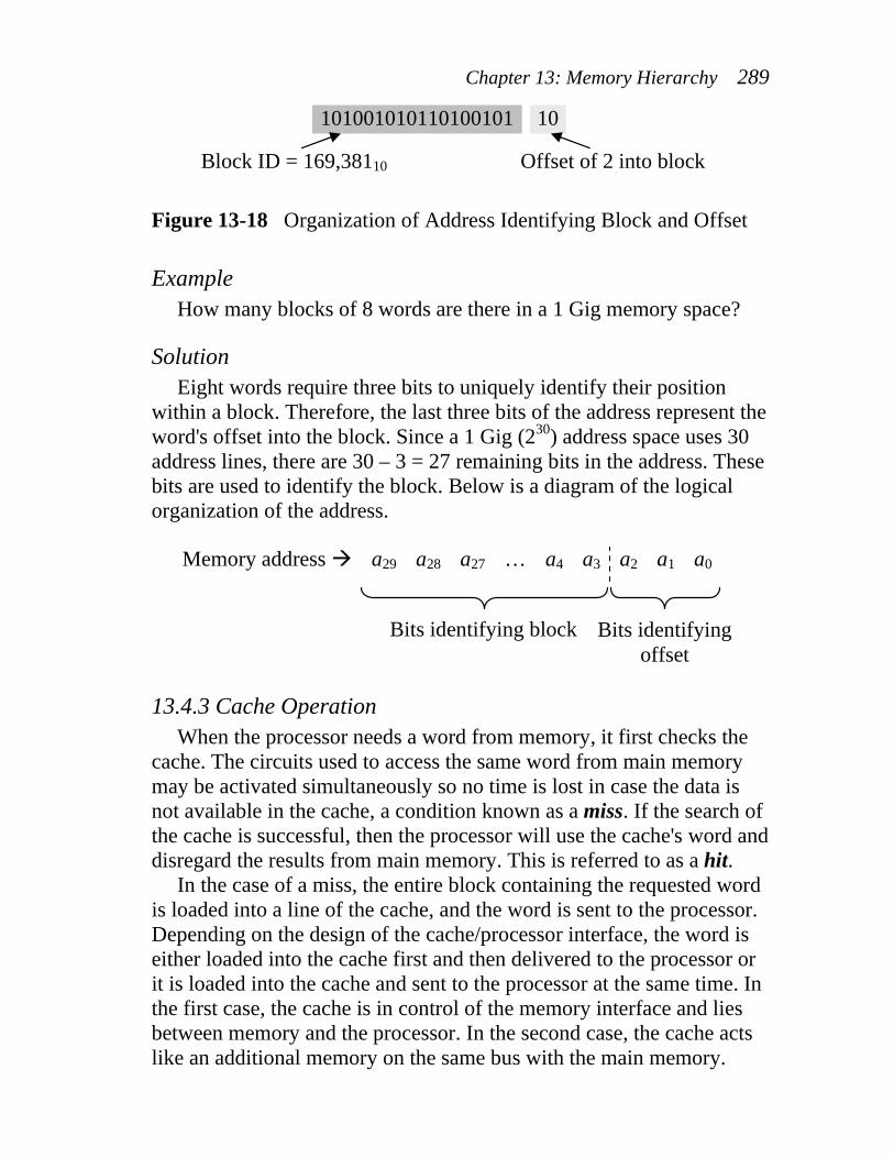
To organize memory into blocks, a memory address is divided into two logical sets of bits, one to represent the block number and one to identify the word's position or offset within the block. The memory address for the example in Figure 13-17 uses the most significant 18 bits to identify the block and the last two bits to identify a word's position within the block. Figure 13-18 presents this division using the address 101001010110100101102 (A569616).
Memory address Data Block identification
0000 0000 0000 0000 00 00 0000 0000 0000 0000 00 01 0000 0000 0000 0000 00 10 0000 0000 0000 0000 00 11
Block 0
0000 0000 0000 0000 01 00 0000 0000 0000 0000 01 01 0000 0000 0000 0000 01 10 0000 0000 0000 0000 01 11
Block 1
0000 0000 0000 0000 10 00 0000 0000 0000 0000 10 01 0000 0000 0000 0000 10 10 0000 0000 0000 0000 10 11
Block 2
1111 1111 1111 1111 11 00 1111 1111 1111 1111 11 01 1111 1111 1111 1111 11 10 1111 1111 1111 1111 11 11
Block 2(20-2) – 1 = 262,143
Each gray block represents an addressable memory location containing a word
Chapter 13: Memory Hierarchy 289
Figure 13-18 Organization of Address Identifying Block and Offset
Example How many blocks of 8 words are there in a 1 Gig memory space?
Solution Eight words require three bits to uniquely identify their position
within a block. Therefore, the last three bits of the address represent the word's offset into the block. Since a 1 Gig (230) address space uses 30 address lines, there are 30 – 3 = 27 remaining bits in the address. These bits are used to identify the block. Below is a diagram of the logical organization of the address.
13.4.3 Cache Operation When the processor needs a word from memory, it first checks the
cache. The circuits used to access the same word from main memory may be activated simultaneously so no time is lost in case the data is not available in the cache, a condition known as a miss. If the search of the cache is successful, then the processor will use the cache's word and disregard the results from main memory. This is referred to as a hit.
In the case of a miss, the entire block containing the requested word is loaded into a line of the cache, and the word is sent to the processor. Depending on the design of the cache/processor interface, the word is either loaded into the cache first and then delivered to the processor or it is loaded into the cache and sent to the processor at the same time. In the first case, the cache is in control of the memory interface and lies between memory and the processor. In the second case, the cache acts like an additional memory on the same bus with the main memory.
101001010110100101
Block ID = 169,38110
10
Offset of 2 into block
Memory address a29 a28 a27 … a4 a3 a2 a1 a0
Bits identifying block Bits identifying
offset

290 Computer Organization and Design Fundamentals
13.4.4 Cache Characteristics The cache system used by a processor is defined by six traits:
• the size of the cache; • the size of a block, which when combined with the size of the cache
defines the number of lines; • the number of caches (i.e., multiple levels or a split cache); • the mapping function (the link between a block's address in
memory and its location in the cache); • the replacement algorithm (the method used to figure out which
block to remove from the cache in order to free up a line); and • the write policy (how the processor writes data to the cache so that
main memory eventually gets updated). As far as the size of a cache is concerned, designers need to perform
a balancing act to determine the best size cache for a system. The larger a cache is, the more likely it is that the processor will find the word it needs in the cache. The problem is that as a cache gets larger, the address decoding circuits also get larger and therefore slower. In addition, more complicated logic is required to search a cache because of the seemingly random way that the blocks are stored in it. Larger caches are also more expensive.
There is also a relationship between size of a block and the performance of the cache. As the block size goes up, the possibility of getting a hit when looking for data could go up due to more words being available within a region of active code. For a fixed cache size, however, as the block size increases, the number of blocks that can be stored in a cache goes down thereby potentially reducing the number of hits. A typical size of a block is fairly low, between 4 and 8 words.
13.4.5 Cache Mapping Functions There are three main methods used to map a line in the cache to an
address in memory so that the processor can quickly find a word: direct mapping, full associative mapping, and set associative mapping. Let's begin with direct mapping.
Assume main memory is divided up into n blocks and the cache has room to contain exactly m blocks. Because of the nature of the cache, m is much smaller than n. If we divide m into n, we should get an integer

Chapter 13: Memory Hierarchy 291
which represents the number of times that the main memory could fill the cache with different blocks from its contents.
For example, if main memory is 128 Meg (227) and a block size is four words (22), then main memory contains n = 227–2 = 225 blocks. If the cache for this system can hold 256 K (218) words, then m = 218–2 = 216 blocks. Therefore, the main memory could fill the cache n/m = 225/216 = 225–16 = 29 = 512 times.
Another way of putting it is this: the memory is much larger than a cache, so each line in the cache is responsible for storing one of many blocks from main memory. In the case of our example above, each line of the cache is responsible for storing one of 512 different blocks from main memory at any one time.
Direct mapping is a method used to assign each memory block in main memory to a specific line in the cache. If a line is already filled with a memory block when a new block needs to be loaded, the old block is discarded from the cache. Figure 13-19 shows how multiple blocks from our example are mapped to each line in the cache.
Figure 13-19 Direct Mapping of Main Memory to Cache
As with locating a word within a block, bits are taken from the main memory address to uniquely define the line in the cache where a block should be stored. For example, if a cache has 29 = 512 lines, then a line would need 9 bits to be uniquely identified. Therefore, the nine bits of the address immediately to the left of the word identification bits would identify the line in the cache where the block is to be stored. The bits of
Memory Block 0 Block 1
Block 512 Block 513
Block 1024 Block 1025
Block 1536 Block 1537
Line 0 Tag0 Block for Tag0 Line 1 Tag1 Block for Tag1 Line 2 Tag2 Block for Tag2 Line 3 Tag3 Block for Tag3
Line 511 Tag511 Block for Tag511
Cache

292 Computer Organization and Design Fundamentals
the address not used for the word offset or the cache line would be used for the tag. Figure 13-20 presents this partitioning of the bits.
Once the block is stored in the line of the cache, the tag is copied to the tag location of the line. From the cache line number, the tag, and the word position within the block, the original address of the word can be reconstructed.
Figure 13-20 Direct Mapping Partitioning of Memory Address
In a nutshell, direct mapping breaks an address into three parts: t tag bits, l line bits, and w word bits. The word bits are the least significant bits identifying the specific word within a block of memory. The line bits are the next least significant identifying in which line of the cache the block will be stored. The remaining bits are stored with the block as the tag identifying where the block is located in main memory.
Example Assume a cache system has been designed such that each block
contains 4 words and the cache has 1024 lines, i.e., the cache can store up to 1024 blocks. What line of the cache is supposed to hold the block that contains the word from the twenty-bit address 3A45616? In addition, what is the tag number that will be stored with the block?
Solution Start by dividing the address into its word id, line id, and tag bits.
Since 4=22, then the two least significant bits identify the word, i.e., w = 2. Since the cache has 1024=210 lines, then the next 10 bits identify the line number where the data is supposed to be stored in the cache, i.e., l = 10. The remaining t = 20 – w – l = 8 bits are the tag bits. This partitions the address 3A45616 = 001110100100010101102 as follows:
00111010 0100010101 10
tag bits line id bits word id bits
t bits l bits w bits
Tag Bits identifyingrow in cache
Bits identifying word offset into block

Chapter 13: Memory Hierarchy 293
Therefore, the block from address 3A45416 to 3A45716 will be stored in line 01000101012 = 27710 of the cache with the tag 001110102.
Example The first 10 lines of a 256 line cache are shown in the table below.
Identify the address of the data that is shaded (D816). For this cache, a block contains 4 words. The tags are given in binary in the table.
Line # Tag word 00 word 01 word 10 word 11
0 110101 12 34 56 78 1 010101 54 32 6A D3 2 000111 29 8C ED F3 3 001100 33 A2 2C C8 4 110011 9A BC D8 F0 5 001101 33 44 55 66 6 010100 92 84 76 68 7 000100 FE ED 00 ED 8 100000 00 11 22 33 9 101000 99 88 77 66
Solution Start by finding the number of bits that represent each part of the
address, i.e., the word id, the line id, and the tag. From the table, we can see that 2 bits represent the positions of each of the four words in a block and that 6 bits are used to represent the tag.
Since the cache has 256=28 lines, then the line number in the cache is represented with 8 bits, and the address is partitioned as follows:
The shaded cell in the table has a tag number of 1100112. The line
number is 4, which in 8 bit binary is 000001002. Last of all, the word is in the third column which means that it is the 102 word within the block. (Remember to start counting from 002.) Putting the tag, line id, and word id bits together gives us:
6 bits 8 bits 2 bits
Tag Bits identifyingrow in cache
Bits identifying wordoffset into block

294 Computer Organization and Design Fundamentals
110011 00000100 10 tag bits line id bits word
id bits
Therefore, the address that the shaded cell containing D816 came from is 1100 1100 0001 00102 = CC1216.
Example Using the table from the previous example, determine if the data
stored in main memory at address 101C16 is contained in this cache, and if it is, retrieve the data.
Solution Converting 101C16 to binary gives us 0001 0000 0001 11002. By
using the breakdown of bits for the tag, line id, and word id, the binary value can be divided into its components.
000100 00000111 00 tag bits line id bits word
id bits From this we see that the line in the cache where this data should be
stored is 000001112 = 710. The tag currently stored in this line is 0001002 which equals the tag from the above partitioned address. Therefore, the data from main memory address 101C16 is stored in this cache. If the stored tag did not match the tag pulled from the address, we would have known that the cache did not contain our address.
Lastly, we can find the data by looking at the offset 002 into the block at line 7. This gives us the value FE16.
Example Using the same table from the previous two examples, determine if
the data from address 982716 is in the cache.
Solution Converting the hexadecimal address 982716 to binary gives us
982716 = 1001 1000 0010 01112. By using the breakdown of bits for the tag, line id, and word id, we can divide this value into its components.

Chapter 13: Memory Hierarchy 295
100110 00001001 11 tag bits line id bits word
id bits From this we see that the tag is 1001102, the line number is
000010012 = 910, and the word offset into the block is 112. Looking at line number 9 we see that the tag stored there equals 1010002. Since this does not equal 1001102, the data from that address is not contained in this cache, and we will have to get it from the main memory.
Fully associative mapping does not use line numbers at all. It
divides the main memory address into two parts: the word id and a tag. In order to see if a block is stored in memory, the tag is pulled from the memory address and a search is performed through all of the lines of the cache to see if the block is present.
Figure 13-21 Fully Associative Partitioning of Memory Address
This method of searching for a block within a cache sounds like it might be a slow process, but it is not. Each line of the cache contains its own compare circuitry that is able to discern in an instant whether or not the block is contained at that line. With all of the lines performing this compare in parallel, the correct line is identified quickly.
This mapping algorithm is meant to solve a problem that occurs with direct mapping where two active blocks of memory map to the same line of the cache. When this happens, neither block of memory is allowed to stay in the cache long before it is replaced by the competing block. This results in a condition referred to as thrashing where a line in the cache goes back and forth between two or more blocks, usually replacing a block before the processor was through with it. Thrashing is avoided by allowing a block of memory to map to any line of the cache.
This benefit has a price, however. When a fully associative cache is full and the processor needs to load a new block from memory, a decision has to be made regarding which of the existing blocks is to be discarded. The selection method, known as a replacement algorithm,
t bits w bits
Tag Bits identifying word
offset into block

296 Computer Organization and Design Fundamentals
should have a goal of replacing the block least likely to be needed by the processor in the near future.
There are numerous replacement algorithms, no one of which is significantly better then the others. In an effort to realize the fastest operation, each of these algorithms is implemented in hardware.
• Least Recently Used (LRU) – This method replaces the block that
hasn't been read by the processor in the longest period of time. • First In First Out (FIFO) – This method replaces the block that
has been in cache the longest. • Least Frequently Used (LFU) – This method replaces the block
which has had fewest hits since being loaded into the cache. • Random – This method randomly selects a block to be replaced. It
has only slightly lower performance than LRU, FIFO, or LFU.
Example The table below represents five lines from a cache that uses fully
associative mapping with a block size of eight. Identify the address of the shaded data (C916).
Word id bits (in binary)
Tag 000 001 010 011 100 101 110 111 01101101100102 16 36 66 28 A1 3B D6 78 01000110101012 54 C9 6A 63 54 32 00 D3 00010001110112 29 8C ED FD 29 54 12 F3 00011110011002 39 FA B5 C1 33 9E 33 C8 10011001011012 23 4C D2 40 6A 76 A3 F0
Solution The tag for C916 is 01000110101012. When combining this with the
word id of 0012, the address in main memory from which C916 was retrieved is 01000110101010012 = 46A916.
Example Is the data from memory address 1E6516 contained in the table from
the previous example?

Chapter 13: Memory Hierarchy 297
Solution For this cache, the last three bits identify the word and the rest of the
bits act as the tag. Since 1E6516 = 00011110011001012, then 1012 is the word id and 00011110011002 is the tag. Scanning the rows shows that the fourth row contains this tag, and therefore the table contains the data in which we are interested. The word identified by 1012 is 9E16.
The last mapping algorithm presented here is set associative
mapping. Set associative mapping combines direct mapping with fully associative mapping by grouping together lines of a cache into sets. The sets are identified using a direct mapping scheme while the lines within each set are treated like a miniature fully associative cache where any block that is to be stored in the set can be stored to any line within the set. Figure 13-22 represents this arrangement with a sample cache that uses four lines to a set.
Figure 13-22 Set Associative Mapping of Main Memory to Cache
A set associative cache that has k lines per set is referred to as a k-way set associative cache. Since the mapping scheme uses the memory address just as direct mapping does, the number of lines contained in a set must be equal to an integer power of two, e.g., two, four, eight, sixteen, and so on.
Let's use an example to further explain set associative mapping. Assume that a system uses a cache with 29 = 512 lines, a block of memory contains 23 = 8 words, and the full memory space contains 230 = 1 Gig words. In a direct mapping scheme, this would leave 30 – 9 – 3
Memory Block 0 Block 1
Block 128 Block 129
Block 256 Block 257
Block 384 Block 385
Tag0 Block for Tag0 Tag1 Block for Tag1 Tag2 Block for Tag2 Tag3 Block for Tag3
Tag511 Block for Tag511
Cache
Tag4 Block for Tag4 Tag5 Block for Tag5 Tag6 Block for Tag6 Tag7 Block for Tag7 Tag8 Block for Tag8
Set 0
Set 1

298 Computer Organization and Design Fundamentals
= 18 bits for the tag. Note that the direct mapping method is equivalent to the set associative method where the set size is equal to one line.
By going from direct mapping to set associative with a set size of two lines per set, the number of sets is equal to half the number of lines. In the case of the cache with 512 lines, that would give us 256 sets of two lines each which would require eight bits from the memory address to identify the set. This would leave 30 – 8 – 3 = 19 bits for the tag. By going to four lines per set, the number of sets is reduced to 128 sets requiring seven bits to identify the set and twenty bits for the tag.
Figure13-23 shows how each time the number of lines per set in the example is doubled, the number of bits used to identify the set is reduced by one thereby increasing the number of tag bits by one.
Figure 13-23 Effect of Cache Set Size on Address Partitioning
When a block from memory needs to be stored to a set already filled with other blocks, one of the replacement algorithms described for fully associative mapping is used. For a 2-way set associative cache, one of the easiest replacement algorithms to implement is the least recently used method. Each set contains a single bit identifying which of the two lines was used last. If the bit contains a zero, then the first line was used last and the second line is the one that should be replaced. If the bit contains a one, the first line should be replaced.
Example Identify the set number where the block containing the address
29ABCDE816 will be stored. In addition, identify the tag and the lower
Tag bits Set ID bits Word
ID bits
18 bits 9 bits 3 bits Direct mapping (1 line/set) 19 bits 8 bits 3 bits 2-way set associative (21 lines/set) 20 bits 7 bits 3 bits 4-way set associative (22 lines/set) 21 bits 6 bits 3 bits 8-way set associative (23 lines/set)
25 bits 2 bits 3 bits 128-way set associative (27 lines/set)26 bits 1 bit 3 bits 256-way set associative (28 lines/set)
27 bits 3 bits Fully associative (1 big set)

Chapter 13: Memory Hierarchy 299
and upper addresses of the block. Assume the cache is a 4-way set associative cache with 4K lines, each block containing 16 words, with the main memory of size 1 Gig memory space.
Solution First, we need to identify the partitioning of the bits in the memory
address. A 1 Gig memory space requires 30 address lines. Four of those address lines will be used to identify one out of the 16 words within the block. Since the cache is a 4-way set associative cache, the number of sets equals 4K lines divided by four lines per set, i.e., 1K = 210. Therefore, ten address lines will be needed to identify the set. The figure below represents the partitioning of the 30 bit address.
Converting 29ABCDE816 to a 30-bit binary value gives us
001010011010101111001101111010002. The first sixteen bits, 0010100110101011112, represent the tag. The next ten bits, 00110111102 = 22210, represent the set in which the block will be stored. The last four bits, 10002 = 810, represent the word position within the block. The lowest address will be the one where word 00002 is stored and the highest address will be the one where the word 11112 is stored. Replacing the last four bits of 29ABCDE816 with 00002 gives us a low address of 29ABCDE016 while replacing them with 11112 gives us a high address of 29ABCDEF16
13.4.6 Cache Write Policy The last characteristic of caches discussed here is the cache write
policy, i.e., the method used to determine how memory is updated when the cache is written to by the processor. There are a number of issues surrounding this topic, most of which apply to multi-processor systems which are beyond the scope of this text. Basically, when the cache is written to, the corresponding location in memory becomes obsolete.
One method for resolving this is to have the cache update memory every time the processor writes to the cache. This is called a write through policy. The problem with this is that it creates a great deal of
16 bits 10 bits 4 bits
Tag Bits identifyingthe set in cache
Bits identifying wordoffset into block

300 Computer Organization and Design Fundamentals
memory bus traffic, some of which might be unnecessary if the same memory location is being updated often. This policy also slows the write process since both memories are being updated at the same time.
A second method is to update main memory only when a line of the cache that has been modified to is about to be replaced with a new block from memory. This is called a write back policy. This method runs into problems when more than one processor such as an I/O processor is sharing memory. Solutions include making shared memory non-cacheable, adding an additional processor to watch all of the caches and make appropriate updates when a write occurs, or giving all of the processors the ability to check other caches for updates.
13.5 Registers At the top of the memory hierarchy is a set of memory cells called
registers. A register is a group of latches that have been combined in order to perform a special purpose. This group of latches may be used to store an integer, store an address pointing to memory, configure an I/O device, or indicate the status of a process. Whatever the purpose of the register is, all of the bits are treated as a unit.
Registers are contained inside the processor and are integrated with the circuitry used to perform the processor's internal operations. This integration places registers within millionths of a meter of the action resulting in very quick access times. In addition, the typical processor contains fewer than a hundred registers making decoding very simple and very fast. These two features combine to make registers by far the fastest memory unit in the memory hierarchy.
Because of the integral part they play in computer architecture, the details and applications of registers are presented in Chapter 15.
13.6 What's Next? This chapter presented the system of memory components that serve
the processor. This system will be revisited in Chapter 15 where a detailed examination of the organization of the components inside of the processor will be introduced.
Chapter 14 presents another important component supporting the processor: serial communications. Up to this point, our discussion of the processor has used the parallel bus to transfer data. The parallel bus has some drawbacks though. These include higher expense, lack of adaptability, and lower reliability. Chapter 14 presents the basic

Chapter 13: Memory Hierarchy 301
structure of a serial communications system followed by a presentation of two serial protocols.
Problems 1. Why is it important for hard drive substrates to be rigid?
2. Why is it important for hard drive substrates to be lightweight?
3. What is the advantage of a Winchester head, and how is it achieved?
4. Sketch the pattern of magnetic polarity found using the RLL encoding of Figure 13-5 for the bit pattern 0110100110100110101.
5. Calculate the amount of time it would take to read a 2 Mbyte file from a 15,000 RPM drive with a typical 4 ms seek time that has 500 sectors per track each of which contains 512 bytes. Assume the file is stored sequentially and take into account the delays incurred each time the drive must switch tracks.
6. Repeat the previous problem assuming the sectors of the file are scattered randomly across the tracks of the platters.
7. How many blocks of 16 words are there in a 256 Gig memory space? Draw the logical organization of the full address identifying the block ID portion and the word offset portion.
8. Identify the line number, tag, and word position for each of the 30-bit addresses shown below if they are stored in a cache using the direct mapping method.
a.) Address: 23D94EA616 Lines in cache: 4K Block size: 2 b.) Address: 1A54387F6 Lines in cache: 8K Block size: 4 c.) Address: 3FE9704A16 Lines in cache: 16K Block size: 16 d.) Address: 54381A516 Lines in cache: 1K Block size: 8
9. True or False: A block from main memory could possibly be
stored in any line of a cache using fully associative mapping.
10. What problem is the fully or set-associative mapping methods for caches supposed to solve over the direct mapping method?
11. What is the easiest replacement algorithm to use with a 2-way set associative cache?

302 Computer Organization and Design Fundamentals
12. The table below represents five lines from a cache that uses fully associative mapping with a block size of eight. Identify the address of the shaded data (3B16).
Word id bits (in binary) Tag 000 001 010 011 100 101 110 111
100110110110001012 10 65 BA 0F C4 19 6E C3 001110000110101012 21 76 CB 80 D5 2A 7F B5 101111000101110012 32 87 DC 91 E6 3B F0 A6 011101100011010112 43 98 ED A2 F7 4C E1 97 001111001001110002 54 9A FE B3 08 5D D2 88
13. Using the table from the previous problem, identify the data value
represented by each of the following addresses.
a.) 7635916 b.) 386AF16 c.) BC5CC16
14. Identify the set number, tag, and word position for each of the 30-bit addresses stored in an 8K line set associative cache.
a.) Address: 23D94EA616 2-way cache Block size: 2 b.) Address: 1A54387F6 2-way cache Block size: 4 c.) Address: 3FE9704A16 8-way cache Block size: 16 d.) Address: 54381A516 4-way cache Block size: 8
15. Using the C declarations below of a simulated 256 line cache and a
64K memory, create two functions. The first function, bool requestMemoryAddress(unsigned int address), takes as its parameter a 16-bit value and checks to see if it exists in the cache. If it does, simply return a value of TRUE. If it doesn't, load the appropriate line of the cache with the requested block from memory[] and return a FALSE. The second function, unsigned int getPercentageOfHits(void), should return an integer from 0 to 100 representing the percentage of successful hits in the cache. typedef struct { int tag; char block[4]; }cache_line;
cache_line cache[256];
char memory[65536];