1 registers and counters ee 208 – logic design chapter 6 sohaib majzoub
TRANSCRIPT
1
Registers and CountersRegisters and Counters
EE 208 – Logic Design
Chapter 6
Sohaib Majzoub
2
Latches, Flip-flops and RegistersLatches, Flip-flops and Registers
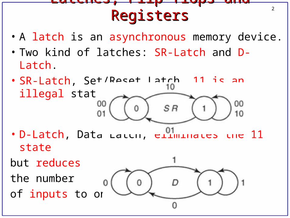
• A latch is an asynchronous memory device.
• Two kind of latches: SR-Latch and D-Latch.
• SR-Latch, Set/Reset Latch, 11 is an illegal state:
• D-Latch, Data Latch, eliminates the 11 state
but reduces
the number
of inputs to one
3
Latches, Flip-flops and RegistersLatches, Flip-flops and Registers
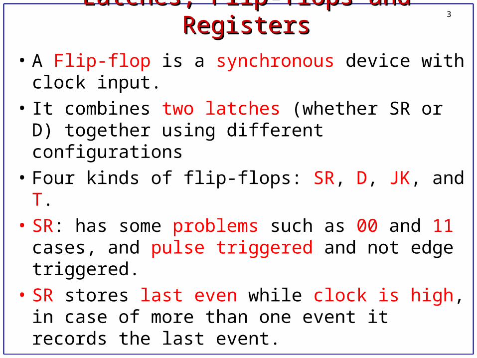
• A Flip-flop is a synchronous device with clock input.
• It combines two latches (whether SR or D) together using different configurations
• Four kinds of flip-flops: SR, D, JK, and T.
• SR: has some problems such as 00 and 11 cases, and pulse triggered and not edge triggered.
• SR stores last even while clock is high, in case of more than one event it records the last event.
4Latches, Flip-flops and RegistersLatches, Flip-flops and Registers
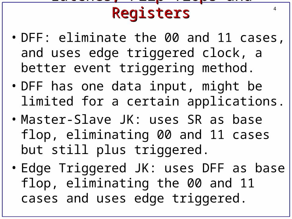
• DFF: eliminate the 00 and 11 cases, and uses edge triggered clock, a better event triggering method.
• DFF has one data input, might be limited for a certain applications.
• Master-Slave JK: uses SR as base flop, eliminating 00 and 11 cases but still plus triggered.
• Edge Triggered JK: uses DFF as base flop, eliminating the 00 and 11 cases and uses edge triggered.
5Latches, Flip-flops and RegistersLatches, Flip-flops and Registers
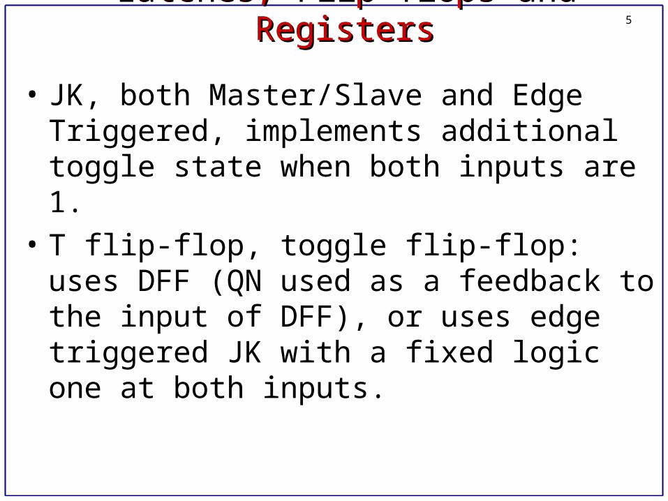
• JK, both Master/Slave and Edge Triggered, implements additional toggle state when both inputs are 1.
• T flip-flop, toggle flip-flop: uses DFF (QN used as a feedback to the input of DFF), or uses edge triggered JK with a fixed logic one at both inputs.
6
Latches, Flip-flops and RegistersLatches, Flip-flops and Registers
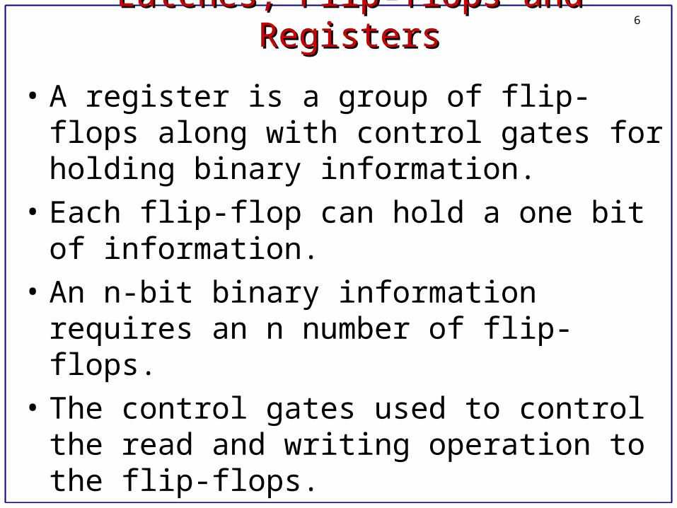
• A register is a group of flip-flops along with control gates for holding binary information.
• Each flip-flop can hold a one bit of information.
• An n-bit binary information requires an n number of flip-flops.
• The control gates used to control the read and writing operation to the flip-flops.
7DFF as Storing DeviceDFF as Storing Device
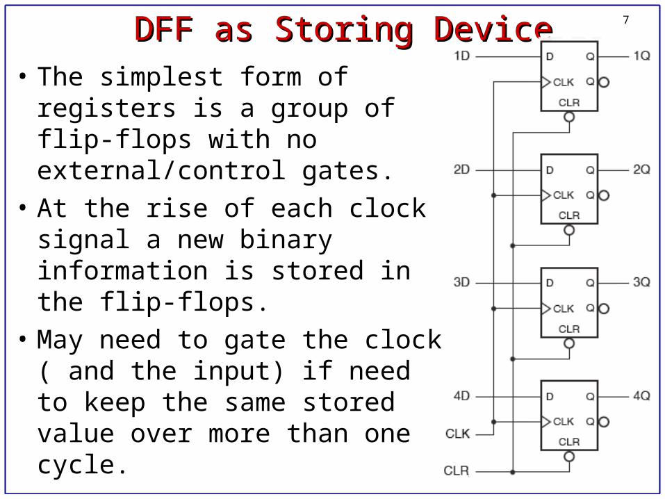
• The simplest form of registers is a group of flip-flops with no external/control gates.
• At the rise of each clock signal a new binary information is stored in the flip-flops.
• May need to gate the clock ( and the input) if need to keep the same stored value over more than one cycle.
8Registers (using DFF)Registers (using DFF)
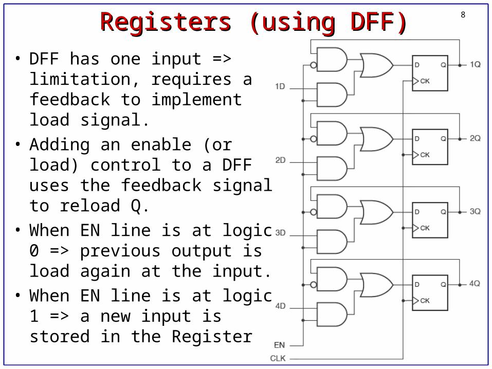
• DFF has one input => limitation, requires a feedback to implement load signal.
• Adding an enable (or load) control to a DFF uses the feedback signal to reload Q.
• When EN line is at logic 0 => previous output is load again at the input.
• When EN line is at logic 1 => a new input is stored in the Register
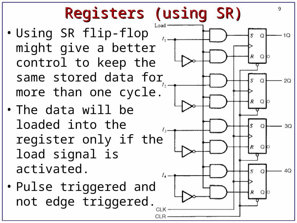
9Registers (using SR)Registers (using SR)• Using SR flip-flop might
give a better control to keep the same stored data for more than one cycle.
• The data will be loaded into the register only if the load signal is activated.
• Pulse triggered and not edge triggered.
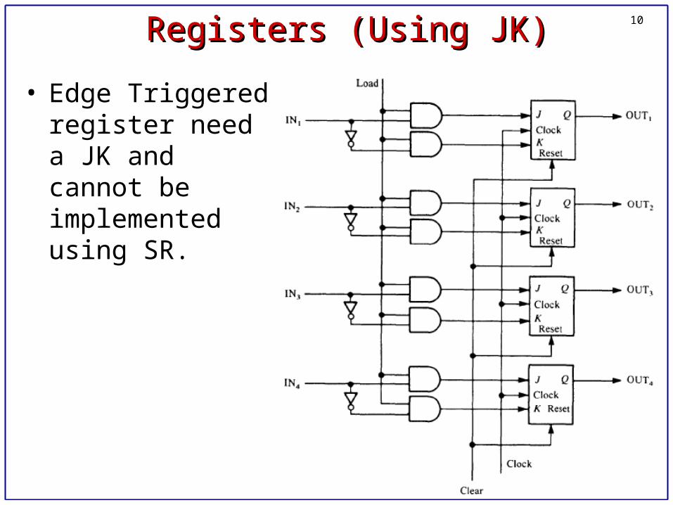
10Registers (Using JK)Registers (Using JK)
• Edge Triggered register need a JK and cannot be implemented using SR.
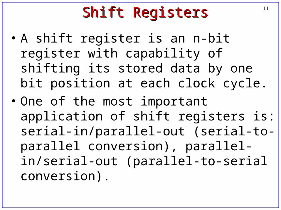
11Shift RegistersShift Registers
• A shift register is an n-bit register with capability of shifting its stored data by one bit position at each clock cycle.
• One of the most important application of shift registers is: serial-in/parallel-out (serial-to-parallel conversion), parallel-in/serial-out (parallel-to-serial conversion).
12
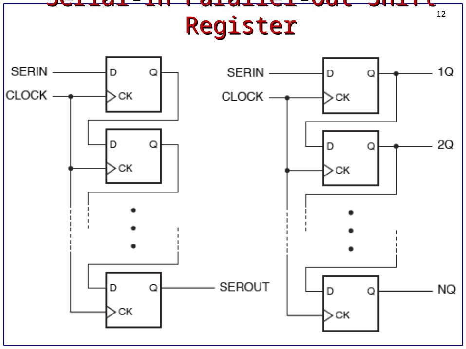
Serial-In Parallel-Out Shift RegisterSerial-In Parallel-Out Shift Register
13
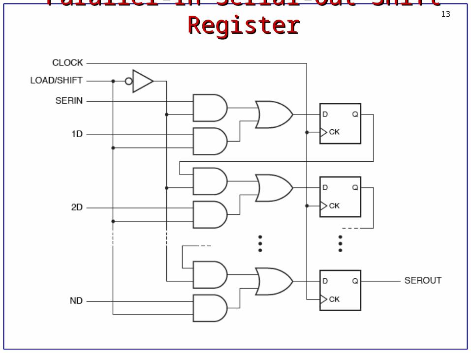
Parallel-In Serial-Out Shift RegisterParallel-In Serial-Out Shift Register
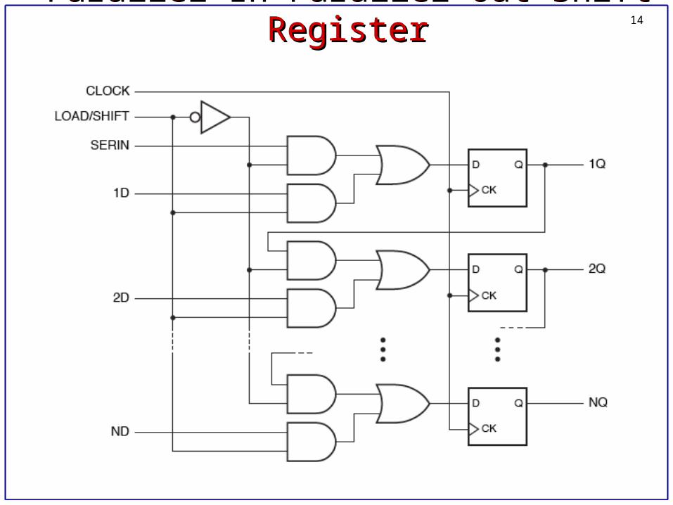
14Parallel-In Parallel-Out Shift RegisterParallel-In Parallel-Out Shift Register
15
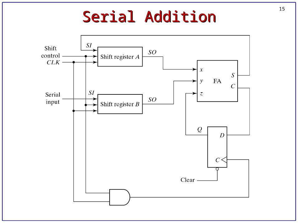
Serial Addition Serial Addition
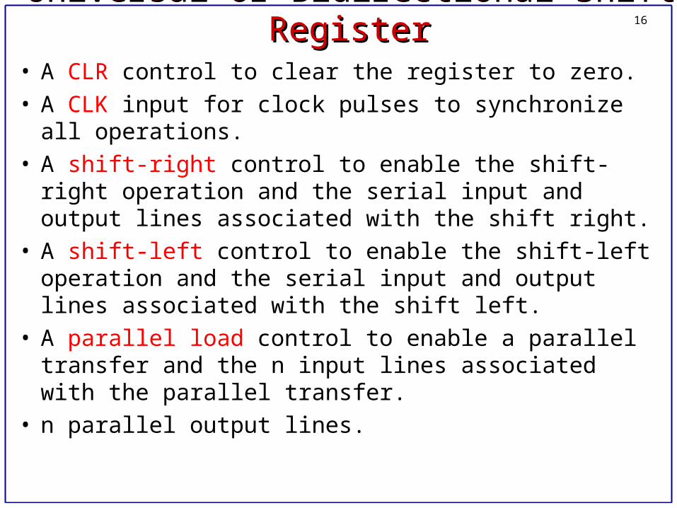
16Universal or Bidirectional Shift RegisterUniversal or Bidirectional Shift Register• A CLR control to clear the register to zero.• A CLK input for clock pulses to synchronize all
operations.• A shift-right control to enable the shift-right operation
and the serial input and output lines associated with the shift right.
• A shift-left control to enable the shift-left operation and the serial input and output lines associated with the shift left.
• A parallel load control to enable a parallel transfer and the n input lines associated with the parallel transfer.
• n parallel output lines.
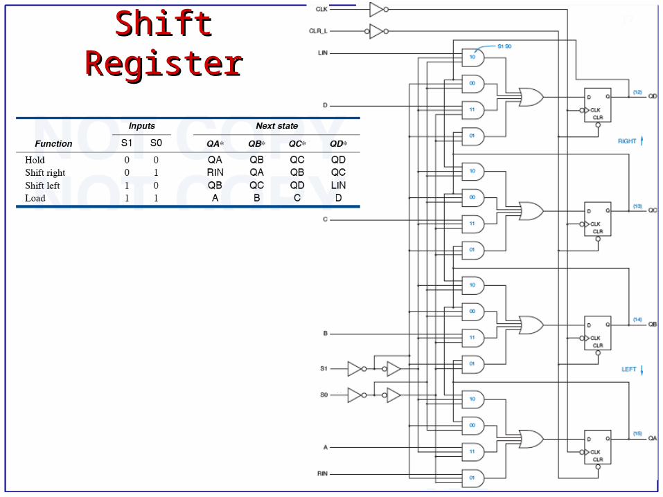
17Universal Shift Universal Shift RegisterRegister
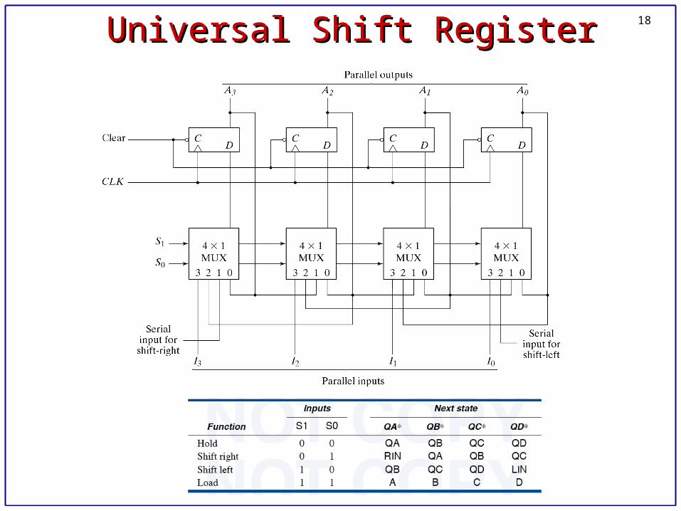
18Universal Shift RegisterUniversal Shift Register
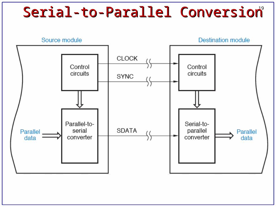
19Serial-to-Parallel ConversionSerial-to-Parallel Conversion
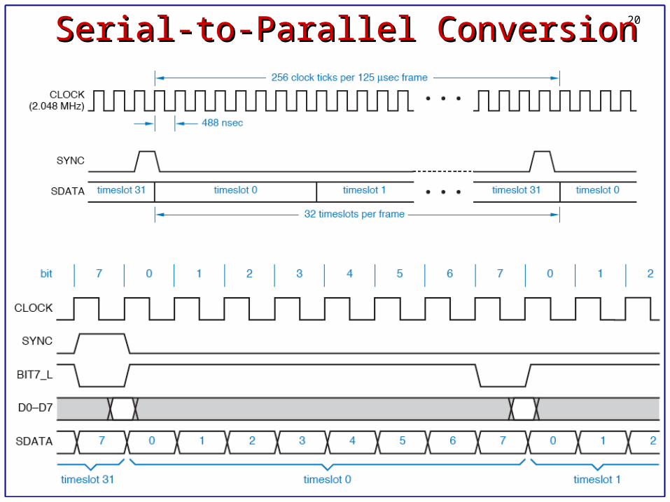
20Serial-to-Parallel ConversionSerial-to-Parallel Conversion
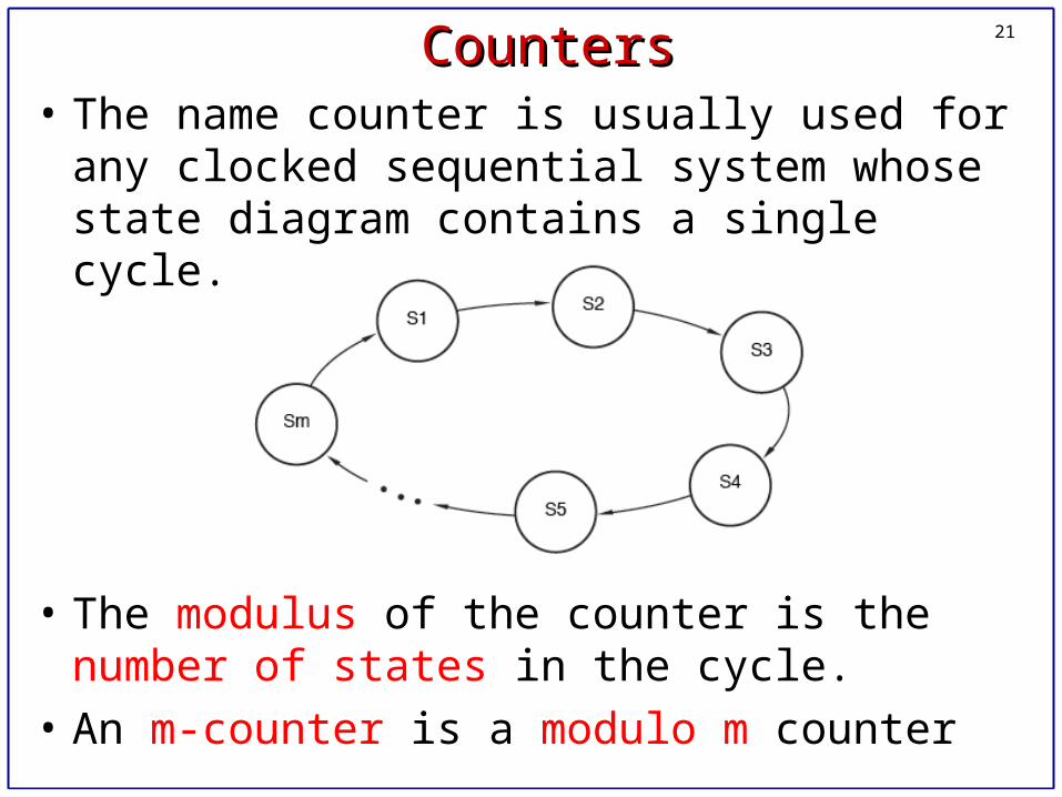
21CountersCounters• The name counter is usually used for any
clocked sequential system whose state diagram contains a single cycle.
• The modulus of the counter is the number of states in the cycle.
• An m-counter is a modulo m counter
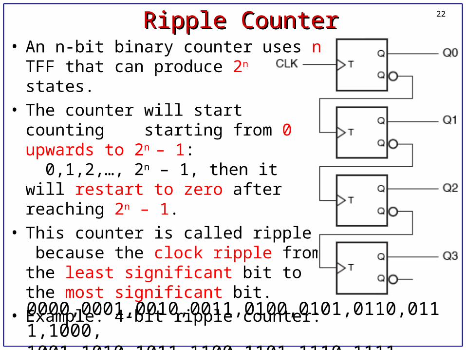
22Ripple CounterRipple Counter• An n-bit binary counter uses n TFF
that can produce 2n states.• The counter will start counting
starting from 0 upwards to 2n – 1: 0,1,2,…, 2n – 1, then it will restart to zero after reaching 2n – 1.
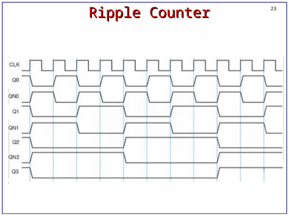
• This counter is called ripple because the clock ripple from the least significant bit to the most significant bit.
• Example: 4-bit ripple counter:
0000,0001,0010,0011,0100,0101,0110,0111,1000, 1001,1010,1011,1100,1101,1110,1111.
23Ripple CounterRipple Counter
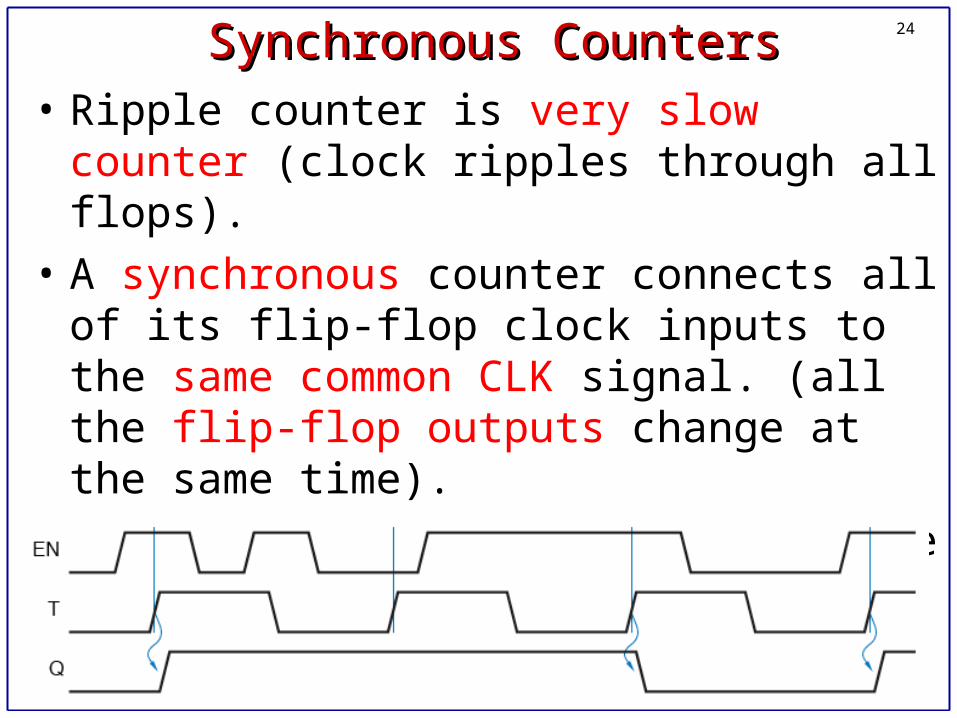
24Synchronous CountersSynchronous Counters• Ripple counter is very slow counter (clock
ripples through all flops).
• A synchronous counter connects all of its flip-flop clock inputs to the same common CLK signal. (all the flip-flop outputs change at the same time).
• An enable line should be used, the output toggles only in EN is 1.
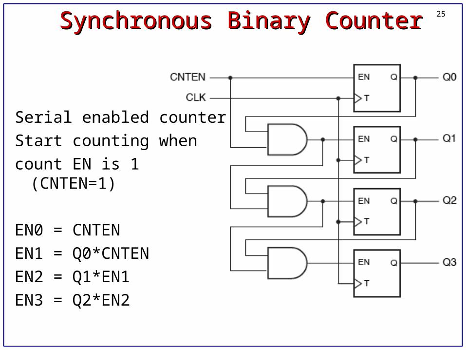
25Synchronous Binary CounterSynchronous Binary Counter
Serial enabled counter
Start counting when
count EN is 1 (CNTEN=1)
EN0 = CNTEN
EN1 = Q0*CNTEN
EN2 = Q1*EN1
EN3 = Q2*EN2
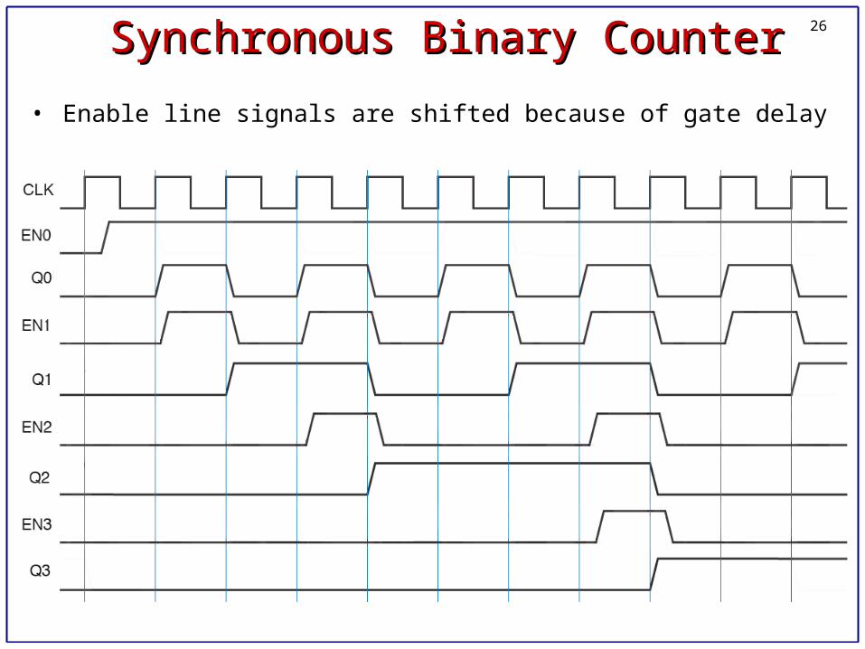
26Synchronous Binary CounterSynchronous Binary Counter
• Enable line signals are shifted because of gate delay
27Synchronous Binary CounterSynchronous Binary Counter
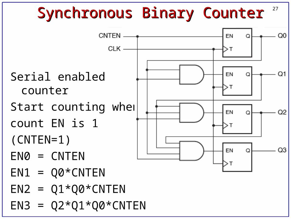
Serial enabled counter
Start counting when
count EN is 1
(CNTEN=1)
EN0 = CNTEN
EN1 = Q0*CNTEN
EN2 = Q1*Q0*CNTEN
EN3 = Q2*Q1*Q0*CNTEN