1 features 2 applications - analog, embedded processing ... · 50 55 60 65 70 75 80 85 90 95 100 0...
TRANSCRIPT
50
55
60
65
70
75
80
85
90
95
100
0 0.5 1 1.5 2 2.5 3
0.8
1.21.51.8
2.53.35.0
25° C
OUTPUT CURRENT(A)
EF
FIC
IEN
CY
(%
)VIN
CIN
10 PF
Enable
RON
See Table RFBT
CFF 0.022 PF
See Table
CSS
0.022 PF
RFBB
See Table100 PF
LMZ12003
VO
UT
FB
RO
N
SS
VIN
EN
GN
D
VOUT @ 3A
Product
Folder
Sample &Buy
Technical
Documents
Tools &
Software
Support &Community
LMZ12003SNVS636O –DECEMBER 2009–REVISED AUGUST 2015
LMZ12003 3-A Simple Switcher® Power Module with 20-V Maximum Input Voltage1 Features 2 Applications1• Integrated Shielded Inductor • Point-of-load Conversions from 5-V and 12-V
Input Rail• Simple PCB Layout• Time-Critical Projects• Flexible Start-up Sequencing Using External Soft-
start Capacitor and Precision Enable • Space-Constrained High Thermal RequirementApplications• Protection Against Inrush Currents and Faults
such as Input UVLO and Output Short Circuit • Negative Output Voltage Applications(See AN-2027) SNVA425• Junction Temperature Range –40°C to 125°C
• Single Exposed Pad and Standard Pinout for Easy 3 DescriptionMounting and ManufacturingThe LMZ12003 SIMPLE SWITCHER® power module• Fast Transient Response for FPGAs and ASICs is an easy-to-use step-down DC-DC solution capable
• Low Output Voltage Ripple of driving up to 3-A load with exceptional powerconversion efficiency, line and load regulation, and• Pin-to-Pin Compatible With Devices:output accuracy. The LMZ12003 is available in an– LMZ14203/2/1 (42-V Maximum 3 A, 2 A, 1 A)innovative package that enhances thermal
– LMZ12003/2/1 (20-V Maximum 3 A, 2 A, 1 A) performance and allows for hand or machine• Fully WEBENCH® Power Designer Enabled soldering.• Electrical Specifications The LMZ12003 can accept an input voltage rail
between 4.5 V and 20 V and can deliver an– 18-W Maximum Total Power Outputadjustable and highly accurate output voltage as low– Up to 3-A Output Currentas 0.8 V. The LMZ12003 only requires three external
– Input Voltage Range 4.5 V to 20 V resistors and four external capacitors to complete the– Output Voltage Range 0.8 V to 6 V power solution. The LMZ12003 is a reliable and
robust design with the following protection features:– Efficiency up to 92%thermal shutdown, input undervoltage lockout, output• Performance Benefits overvoltage protection, short circuit protection, output
– Operates at High Ambient Temperature With current limit, and this device allows start-up into aNo Thermal Derating prebiased output. A single resistor adjusts the
switching frequency up to 1 MHz.– High Efficiency Reduces System HeatGeneration Device Information(1)(2)
– Low Radiated Emissions (EMI) Tested to PART NUMBER PACKAGE BODY SIZE (NOM)EN55022 Class B StandardLMZ12003 NDW (7) 9.85 mm × 10.16 mm
– Passes 10-V/m Radiated Immunity EMI Test(1) For all available packages, see the orderable addendum atStandard EN61000 4-3 the end of the data sheet.(2) Peak reflow temperature equals 245°C. See SNAA214 for
more details.
Simplified Application Schematic Efficiency 12-V Input at 25°C
1
An IMPORTANT NOTICE at the end of this data sheet addresses availability, warranty, changes, use in safety-critical applications,intellectual property matters and other important disclaimers. PRODUCTION DATA.
LMZ12003SNVS636O –DECEMBER 2009–REVISED AUGUST 2015 www.ti.com
Table of Contents1 Features .................................................................. 1 8 Application and Implementation ........................ 11
8.1 Application Information............................................ 112 Applications ........................................................... 18.2 Typical Application ................................................. 113 Description ............................................................. 1
9 Power Supply Recommendations ...................... 174 Revision History..................................................... 210 Layout................................................................... 175 Pin Configuration and Functions ......................... 3
10.1 Layout Guidelines ................................................. 176 Specifications......................................................... 310.2 Layout Examples................................................... 186.1 Absolute Maximum Ratings ..................................... 310.3 Power Dissipation and Thermal Considerations... 196.2 ESD Ratings.............................................................. 310.4 Power Module SMT Guidelines ............................ 206.3 Recommended Operating Conditions....................... 4
11 Device and Documentation Support ................. 216.4 Thermal Information .................................................. 411.1 Device Support...................................................... 216.5 Electrical Characteristics........................................... 411.2 Documentation Support ........................................ 216.6 Typical Characteristics ............................................. 611.3 Community Resources.......................................... 217 Detailed Description .............................................. 911.4 Trademarks ........................................................... 217.1 Overview ................................................................... 911.5 Electrostatic Discharge Caution............................ 217.2 Functional Block Diagram ......................................... 911.6 Glossary ................................................................ 217.3 Feature Description................................................... 9
12 Mechanical, Packaging, and Orderable7.4 Device Functional Modes........................................ 10Information ........................................................... 22
4 Revision HistoryNOTE: Page numbers for previous revisions may differ from page numbers in the current version.
Changes from Revision N (October 2013) to Revision O Page
• Added ESD Ratings table, Feature Description section, Device Functional Modes, Application and Implementationsection, Power Supply Recommendations section, Layout section, Device and Documentation Support section, andMechanical, Packaging, and Orderable Information section. ................................................................................................ 1
Changes from Revision M (March 2013) to Revision N Page
• Deleted 12 mils....................................................................................................................................................................... 4• Changed 10 mils................................................................................................................................................................... 17• Changed 10 mils................................................................................................................................................................... 20• Added Power Module SMT Guidelines................................................................................................................................. 20
2 Submit Documentation Feedback Copyright © 2009–2015, Texas Instruments Incorporated
Product Folder Links: LMZ12003
LMZ12003www.ti.com SNVS636O –DECEMBER 2009–REVISED AUGUST 2015
5 Pin Configuration and Functions
NDW Package7-Pin
Top View
Pin FunctionsPIN
TYPE DESCRIPTIONNAME NO.
Enable — Input to the precision enable comparator. Rising threshold is 1.18-V nominal; 90-EN 3 Analog mV hysteresis nominal. Maximum recommended input level is 6.5 V.Exposed Pad — Internally connected to pin 4. Used to dissipate heat from the packageEP — Ground during operation. Must be electrically connected to pin 4 external to the package.Feedback — Internally connected to the regulation, overvoltage, and short circuit
FB 6 Analog comparators. The regulation reference point is 0.8 V at this input pin. Connected thefeedback resistor divider between the output and ground to set the output voltage.
GND 4 Ground Ground — Reference point for all stated voltages. Must be externally connected to EP.ON-Time Resistor — An external resistor from VIN to this pin sets the ON-time of theRON 2 Analog application. Typical values range from 25 kΩ to 124 kΩ.Soft-Start — An internal 8-µA current source charges an external capacitor to produce the
SS 5 Analog soft-start function. This node is discharged at 200 µA during disable, overcurrent, thermalshutdown and internal UVLO conditions.Supply input — Nominal operating range is 4.5 V to 20 V. A small amount of internal
VIN 1 Power capacitance is contained within the package assembly. Additional external input capacitanceis required between this pin and exposed pad.Output Voltage — Output from the internal inductor. Connect the output capacitor betweenVOUT 7 Power this pin and exposed pad.
6 Specifications
6.1 Absolute Maximum Ratings (1) (2) (3)
MIN MAX UNITVIN, RON to GND –0.3 25 VEN, FB, SS to GND –0.3 7 VJunction Temperature 150 °CPeak Reflow Case Temperature (30 sec) 245 °CStorage Temperature, Tstg –65 150 °C
(1) Stresses beyond those listed under Absolute Maximum Ratings may cause permanent damage to the device. These are stress ratingsonly, which do not imply functional operation of the device at these or any other conditions beyond those indicated under RecommendedOperating Conditions. Exposure to absolute-maximum-rated conditions for extended periods may affect device reliability.
(2) If Military/Aerospace specified devices are required, please contact the Texas Instruments Sales Office/ Distributors for availability andspecifications.
(3) For soldering specifications, refer to the following document: SNOA549
6.2 ESD RatingsVALUE UNIT
V(ESD) Electrostatic discharge Human body model (HBM), per ANSI/ESDA/JEDEC JS-001 (1) (2) ±2000 V
(1) JEDEC document JEP155 states that 500-V HBM allows safe manufacturing with a standard ESD control process. Manufacturing withless than 500-V HBM is possible with the necessary precautions.
(2) The human body model is a 100pF capacitor discharged through a 1.5 kΩ resistor into each pin. Test method is per JESD-22-114.
Copyright © 2009–2015, Texas Instruments Incorporated Submit Documentation Feedback 3
Product Folder Links: LMZ12003
LMZ12003SNVS636O –DECEMBER 2009–REVISED AUGUST 2015 www.ti.com
6.3 Recommended Operating Conditionsover operating free-air temperature range (unless otherwise noted)
MIN MAX UNITVIN 4.5 20 VEN 0 6.5 VOperation Junction Temperature –40 125 °C
6.4 Thermal InformationLMZ12003
THERMAL METRIC (1) NDW UNIT7 PINS
RθJA 4-layer JEDEC Printed-Circuit-Board, 100 19.3vias, No air flowJunction-to-ambient thermal resistance (2) °C/W
2-layer JEDEC Printed-Circuit-Board, No 21.5air flowRθJC(top) Junction-to-case (top) thermal resistance No air flow 1.9 °C/W
(1) For more information about traditional and new thermal metrics, see the Semiconductor and IC Package Thermal Metrics applicationreport, SPRA953.
(2) RθJA measured on a 1.705-in × 3.0-in 4-layer board, with 1-oz. copper, thirty five thermal vias, no air flow, and 1-W power dissipation.Refer to PCB layout diagrams.
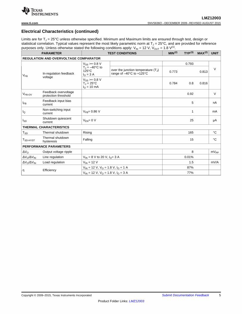
6.5 Electrical CharacteristicsLimits are for TJ = 25°C unless otherwise specified. Minimum and Maximum limits are ensured through test, design orstatistical correlation. Typical values represent the most likely parametric norm at TJ = 25°C, and are provided for referencepurposes only. Unless otherwise stated the following conditions apply: VIN = 12 V, VOUT = 1.8 V (1).
PARAMETER TEST CONDITIONS MIN (2) TYP (3) MAX (2) UNITSYSTEM PARAMETERSENABLE CONTROL
1.18VEN EN threshold trip point VEN rising Vover the junction temperature (TJ) 1.1 1.25range of –40°C to +125°CVEN-HYS EN threshold hysteresis VEN falling 90 mVSOFT-START
8ISS SS source current VSS = 0 V µAover the junction temperature (TJ) 5 11range of –40°C to +125°CISS-DIS SS discharge current –200 µACURRENT LIMIT
4.2DC averageICL Current limit threshold Aover the junction temperature (TJ)VIN= 12 V to 20 V 3.2 5.25range of –40°C to +125°C
ON/OFF TimerON timer minimum pulsetON-MIN 150 nswidth
tOFF OFF timer pulse width 260 ns
(1) EN 55022:2006, +A1:2007, FCC Part 15 Subpart B: 2007. See AN-2024 and layout for information on device under test.(2) Minimum and Maximum limits are 100% production tested at 25°C. Limits over the operating temperature range are ensured through
correlation using Statistical Quality Control (SQC) methods. Limits are used to calculate Average Outgoing Quality Level (AOQL).(3) Typical numbers are at 25°C and represent the most likely parametric norm.
4 Submit Documentation Feedback Copyright © 2009–2015, Texas Instruments Incorporated
Product Folder Links: LMZ12003
LMZ12003www.ti.com SNVS636O –DECEMBER 2009–REVISED AUGUST 2015
Electrical Characteristics (continued)Limits are for TJ = 25°C unless otherwise specified. Minimum and Maximum limits are ensured through test, design orstatistical correlation. Typical values represent the most likely parametric norm at TJ = 25°C, and are provided for referencepurposes only. Unless otherwise stated the following conditions apply: VIN = 12 V, VOUT = 1.8 V(1).
PARAMETER TEST CONDITIONS MIN (2) TYP (3) MAX (2) UNITREGULATION AND OVERVOLTAGE COMPARATOR
VSS >+ 0.8 V 0.793TJ = –40°C to Vover the junction temperature (TJ)125°C 0.773 0.813In-regulation feedback range of –40°C to +125°CIO = 3 AVFB voltageVSS >+ 0.8 VTJ = 25°C 0.784 0.8 0.816IO = 10 mA
Feedback overvoltageVFB-OV 0.92 Vprotection thresholdFeedback input biasIFB 5 nAcurrentNon-switching inputIQ VFB= 0.86 V 1 mAcurrentShutdown quiescentISD VEN= 0 V 25 μAcurrent
THERMAL CHARACTERISTICSTSD Thermal shutdown Rising 165 °C
Thermal shutdownTSD-HYST Falling 15 °ChysteresisPERFORMANCE PARAMETERSΔVO Output voltage ripple 8 mVPP
ΔVO/ΔVIN Line regulation VIN = 8 V to 20 V, IO= 3 A 0.01%ΔVO/ΔVIN Load regulation VIN = 12 V 1.5 mV/A
VIN = 12 V, VO = 1.8 V, IO = 1 A 87%η Efficiency
VIN = 12 V, VO = 1.8 V, IO = 3 A 77%
Copyright © 2009–2015, Texas Instruments Incorporated Submit Documentation Feedback 5
Product Folder Links: LMZ12003
50
55
60
65
70
75
80
85
90
95
100
0 0.5 1 1.5 2 2.5 3
OUTPUT CURRENT (A)
EF
FIC
IEN
CY
(%
)
3.32.5
1.81.51.2
0.8
85°C0
0.5
1
1.5
2
2.5
3
0 0.5 1 1.5 2 2.5 3
OUTPUT CURRENT (A)
DIS
SIP
AT
ION
(W
)
3.32.5
1.8
1.5
1.2
0.8
85°C
50
55
60
65
70
75
80
85
90
95
100
0 0.5 1 1.5 2 2.5 3
0.8
1.21.51.8
2.53.35.0
25° C
OUTPUT CURRENT(A)
EF
FIC
IEN
CY
(%
)
0
0.5
1
1.5
2
2.5
0 0.5 1 1.5 2 2.5 3
OUTPUT CURRENT (A)
DIS
SIP
AT
ION
(W
)
25° C
5.03.32.5
1.8
1.5
0.81.2
LMZ12003SNVS636O –DECEMBER 2009–REVISED AUGUST 2015 www.ti.com
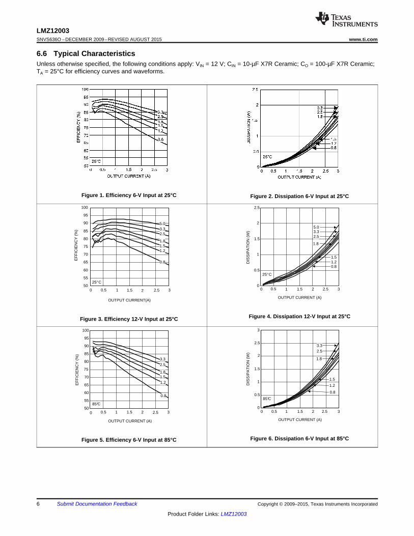
6.6 Typical CharacteristicsUnless otherwise specified, the following conditions apply: VIN = 12 V; CIN = 10-µF X7R Ceramic; CO = 100-µF X7R Ceramic;TA = 25°C for efficiency curves and waveforms.
Figure 1. Efficiency 6-V Input at 25°C Figure 2. Dissipation 6-V Input at 25°C
Figure 4. Dissipation 12-V Input at 25°CFigure 3. Efficiency 12-V Input at 25°C
Figure 6. Dissipation 6-V Input at 85°CFigure 5. Efficiency 6-V Input at 85°C
6 Submit Documentation Feedback Copyright © 2009–2015, Texas Instruments Incorporated
Product Folder Links: LMZ12003
1.8
1.805
1.81
1.815
1.82
1.825
1.83
0 0.5 1 1.5 2 2.5 3
OUTPUT CURRENT (A)
OU
TP
UT
VO
LTA
GE
(V
)
4.5
4.75
5
5.25
5.5
6
1220
25°C
0
0.5
1
1.5
2
2.5
3
0 0.5 1 1.5 2 2.5 3
OUTPUT CURRENT (A)
DIS
SIP
AT
ION
(W
)
5.03.3
2.51.8
1.51.2
0.8
85°C
50
55
60
65
70
75
80
85
90
95
100
0 0.5 1 1.5 2 2.5 3
OUTPUT CURRENT (A)
EF
FIC
IEN
CY
(%
)
5.0
3.32.5
1.81.5
1.2
0.8
85°C
1.5
0
0.5
1
1.5
2
2.5
3
0 0.5 1 1.5 2 2.5 3
OUTPUT CURRENT (A)
DIS
SIP
AT
ION
(W
)
5.0
3.32.5
1.8
1.2
0.8
85°C
50
55
60
65
70
75
80
85
90
95
100
0 0.5 1 1.5 2 2.5 3
OUTPUT CURRENT (A)
EF
FIC
IEN
CY
(%
) 5.03.32.5
1.81.5
1.2
0.8
85°C
LMZ12003www.ti.com SNVS636O –DECEMBER 2009–REVISED AUGUST 2015
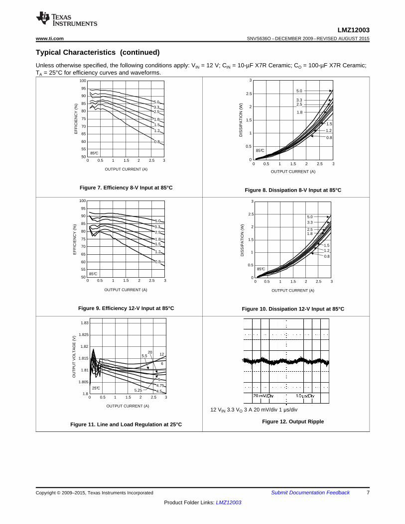
Typical Characteristics (continued)Unless otherwise specified, the following conditions apply: VIN = 12 V; CIN = 10-µF X7R Ceramic; CO = 100-µF X7R Ceramic;TA = 25°C for efficiency curves and waveforms.
Figure 7. Efficiency 8-V Input at 85°C Figure 8. Dissipation 8-V Input at 85°C
Figure 9. Efficiency 12-V Input at 85°C Figure 10. Dissipation 12-V Input at 85°C
12 VIN 3.3 VO 3 A 20 mV/div 1 μs/div
Figure 12. Output RippleFigure 11. Line and Load Regulation at 25°C
Copyright © 2009–2015, Texas Instruments Incorporated Submit Documentation Feedback 7
Product Folder Links: LMZ12003
4.5VIN
0
0.5
1
1.5
2
2.5
3
3.5
50 60 70 80 90 100 110 120
AMBIENT TEMPERATURE (°C)
OU
TP
UT
CU
RR
EN
T (
A)
VOUT = 1.8V
JA = 19.6°C/W
4.5VIN
20VIN
12VIN
LMZ12003SNVS636O –DECEMBER 2009–REVISED AUGUST 2015 www.ti.com
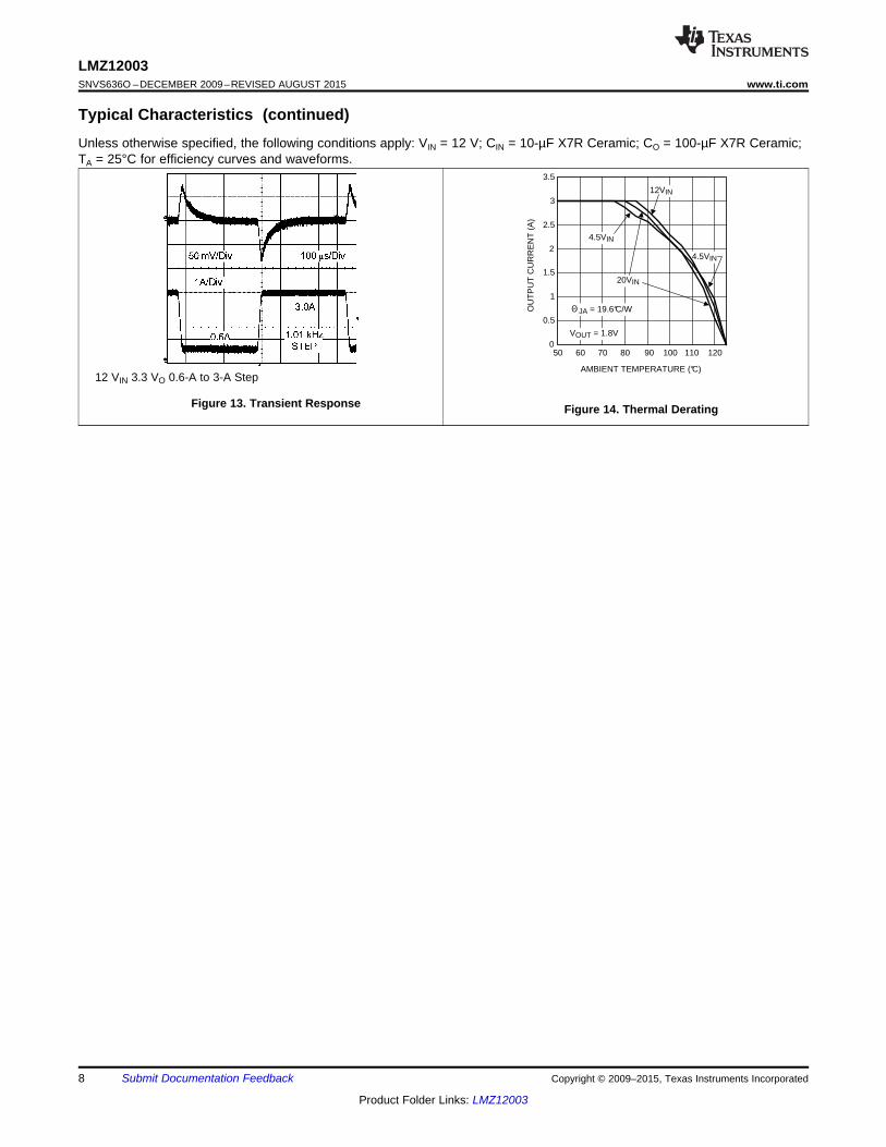
Typical Characteristics (continued)Unless otherwise specified, the following conditions apply: VIN = 12 V; CIN = 10-µF X7R Ceramic; CO = 100-µF X7R Ceramic;TA = 25°C for efficiency curves and waveforms.
12 VIN 3.3 VO 0.6-A to 3-A Step
Figure 13. Transient Response Figure 14. Thermal Derating
8 Submit Documentation Feedback Copyright © 2009–2015, Texas Instruments Incorporated
Product Folder Links: LMZ12003
0.47 éF
6.8 éHCo
CINCvcc
CB
ST
FB
EN
SS
Vin
Linear reg
RONTimer
Css
RON
RFBT
RFBB
CFF
Regulator IC
VO
Internal Passives
VOUT
GND
VIN 1
2
3
4
5
6
7
LMZ12003www.ti.com SNVS636O –DECEMBER 2009–REVISED AUGUST 2015
7 Detailed Description
7.1 OverviewThe LMZ12003 power module is an easy-to-use step-down DC-DC solution capable of driving up to 3-A load withexceptional power conversion efficiency, line and load regulation, and output accuracy.
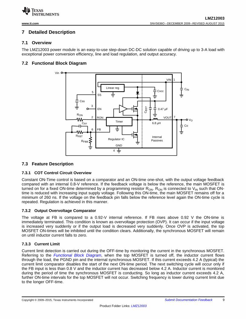
7.2 Functional Block Diagram
7.3 Feature Description
7.3.1 COT Control Circuit OverviewConstant ON-Time control is based on a comparator and an ON-time one-shot, with the output voltage feedbackcompared with an internal 0.8-V reference. If the feedback voltage is below the reference, the main MOSFET isturned on for a fixed ON-time determined by a programming resistor RON. RON is connected to VIN such that ON-time is reduced with increasing input supply voltage. Following this ON-time, the main MOSFET remains off for aminimum of 260 ns. If the voltage on the feedback pin falls below the reference level again the ON-time cycle isrepeated. Regulation is achieved in this manner.
7.3.2 Output Overvoltage ComparatorThe voltage at FB is compared to a 0.92-V internal reference. If FB rises above 0.92 V the ON-time isimmediately terminated. This condition is known as overvoltage protection (OVP). It can occur if the input voltageis increased very suddenly or if the output load is decreased very suddenly. Once OVP is activated, the topMOSFET ON-times will be inhibited until the condition clears. Additionally, the synchronous MOSFET will remainon until inductor current falls to zero.
7.3.3 Current LimitCurrent limit detection is carried out during the OFF-time by monitoring the current in the synchronous MOSFET.Referring to the Functional Block Diagram, when the top MOSFET is turned off, the inductor current flowsthrough the load, the PGND pin and the internal synchronous MOSFET. If this current exceeds 4.2 A (typical) thecurrent limit comparator disables the start of the next ON-time period. The next switching cycle will occur only ifthe FB input is less than 0.8 V and the inductor current has decreased below 4.2 A. Inductor current is monitoredduring the period of time the synchronous MOSFET is conducting. So long as inductor current exceeds 4.2 A,further ON-time intervals for the top MOSFET will not occur. Switching frequency is lower during current limit dueto the longer OFF-time.
Copyright © 2009–2015, Texas Instruments Incorporated Submit Documentation Feedback 9
Product Folder Links: LMZ12003
LMZ12003SNVS636O –DECEMBER 2009–REVISED AUGUST 2015 www.ti.com
Feature Description (continued)
NOTECurrent limit is dependent on both duty cycle and temperature as illustrated in the graphsin the Typical Characteristics section.
7.3.4 Thermal ProtectionThe junction temperature of the LMZ12003 should not be allowed to exceed its maximum ratings. Thermalprotection is implemented by an internal Thermal Shutdown circuit which activates at 165°C (typical) causing thedevice to enter a low power standby state. In this state the main MOSFET remains off causing VO to fall, andadditionally the CSS capacitor is discharged to ground. Thermal protection helps prevent catastrophic failures foraccidental device overheating. When the junction temperature falls back below 145ºC (typical hysteresis = 20°C)the SS pin is released, VO rises smoothly, and normal operation resumes.
Applications requiring maximum output current especially those at high input voltage may require applicationderating at elevated temperatures.
7.3.5 Zero Coil Current DetectionThe current of the lower (synchronous) MOSFET is monitored by a zero coil current detection circuit whichinhibits the synchronous MOSFET when its current reaches zero until the next ON-time. This circuit enables theDCM operating mode, which improves efficiency at light loads.
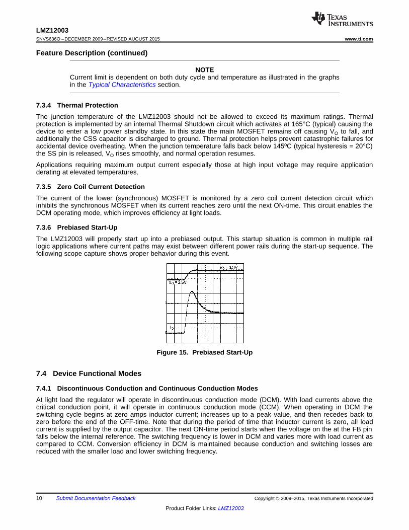
7.3.6 Prebiased Start-UpThe LMZ12003 will properly start up into a prebiased output. This startup situation is common in multiple raillogic applications where current paths may exist between different power rails during the start-up sequence. Thefollowing scope capture shows proper behavior during this event.
Figure 15. Prebiased Start-Up
7.4 Device Functional Modes
7.4.1 Discontinuous Conduction and Continuous Conduction ModesAt light load the regulator will operate in discontinuous conduction mode (DCM). With load currents above thecritical conduction point, it will operate in continuous conduction mode (CCM). When operating in DCM theswitching cycle begins at zero amps inductor current; increases up to a peak value, and then recedes back tozero before the end of the OFF-time. Note that during the period of time that inductor current is zero, all loadcurrent is supplied by the output capacitor. The next ON-time period starts when the voltage on the at the FB pinfalls below the internal reference. The switching frequency is lower in DCM and varies more with load current ascompared to CCM. Conversion efficiency in DCM is maintained because conduction and switching losses arereduced with the smaller load and lower switching frequency.
10 Submit Documentation Feedback Copyright © 2009–2015, Texas Instruments Incorporated
Product Folder Links: LMZ12003
4 5 6 7321
EP
VO
UT
FB
RO
N
SSVIN
EN
GN
D
VIN
CIN2
10 PF
Enable
4.5V to 20V
CFF
0.022 PF
U1
CSS
0.022 PFRFBB
1.07k
LMZ12003TZ-ADJ
1.8VO @ 3A
CO1
1 PFCO2
100 PF
RON
32.4k
RENT
32.4k
RENB
11.8k
RFBT
1.37k
CIN1
1 PF
LMZ12003www.ti.com SNVS636O –DECEMBER 2009–REVISED AUGUST 2015
8 Application and Implementation
NOTEInformation in the following applications sections is not part of the TI componentspecification, and TI does not warrant its accuracy or completeness. TI’s customers areresponsible for determining suitability of components for their purposes. Customers shouldvalidate and test their design implementation to confirm system functionality.
8.1 Application InformationThe LMZ12003 is a step-down DC-to-DC power module. It is typically used to convert a higher DC voltage to alower DC voltage with a maximum output current of 3 A. The following design procedure can be used to selectcomponents for the LMZ12003. Alternately, the WEBENCH software may be used to generate complete designs.
When generating a design, the WEBENCH software uses iterative design procedure and accessescomprehensive databases of components. Please go to www.ti.com for more details.
8.2 Typical Application
Figure 16. Evaluation Board Schematic Diagram
8.2.1 Design RequirementsFor this example the following application parameters exist.• VIN Range = Up to 20 V• VOUT = 0.8 V to 6 V• IOUT = 3 A
8.2.2 Detailed Design ProcedureThe LMZ12003 is fully supported by WEBENCH and offers the following: component selection, electrical andthermal simulations, as well as the build-it board for a reduction in design time. The following list of steps can beused to manually design the LMZ12003 application.
1. Select minimum operating VIN with enable divider resistors2. Program VO with divider resistor selection
Copyright © 2009–2015, Texas Instruments Incorporated Submit Documentation Feedback 11
Product Folder Links: LMZ12003
LMZ12003SNVS636O –DECEMBER 2009–REVISED AUGUST 2015 www.ti.com
Typical Application (continued)3. Program turnon time with soft-start capacitor selection4. Select CO
5. Select CIN
6. Set operating frequency with RON
8.2.2.1 Enable Divider, RENT and RENB SelectionThe enable input provides a precise 1.18-V band-gap rising threshold to allow direct logic drive or connection toa voltage divider from a higher enable voltage such as Vin. The enable input also incorporates 90 mV (typical) ofhysteresis resulting in a falling threshold of 1.09 V. The maximum recommended voltage into the EN pin is 6.5 V.For applications where the midpoint of the enable divider exceeds 6.5 V, a small Zener diode can be added tolimit this voltage.
The function of this resistive divider is to allow the designer to choose an input voltage below which the circuitwill be disabled. This implements the feature of programmable under voltage lockout. This is often used inbattery powered systems to prevent deep discharge of the system battery. It is also useful in system designs forsequencing of output rails or to prevent early turnon of the supply as the main input voltage rail rises at power-up. Applying the enable divider to the main input rail is often done in the case of higher input voltage systemswhere a lower boundary of operation must be established. In the case of sequencing supplies, the divider isconnected to a rail that becomes active earlier in the power-up cycle than the LMZ12003 output rail. The tworesistors must be chosen based on the following ratio:
RENT / RENB = (VIN UVLO / 1.18V) – 1 (1)
The LMZ12003 demonstration and evaluation boards use 11.8 kΩ for RENB and 32.4 kΩ for RENT resulting in arising UVLO of 4.5 V. This divider presents 5.34 V to the EN input when the divider input is raised to 20 V.
The EN pin is internally pulled up to VIN and can be left floating for always-on operation.
8.2.2.2 Output Voltage SelectionOutput voltage is determined by a divider of two resistors connected between VO and ground. The midpoint ofthe divider is connected to the FB input. The voltage at FB is compared to a 0.8-V internal reference. In normaloperation an ON-time cycle is initiated when the voltage on the FB pin falls below 0.8 V. The main MOSFET ON-time cycle causes the output voltage to rise and the voltage at the FB to exceed 0.8 V. As long as the voltage atFB is above 0.8 V, ON-time cycles will not occur.
The regulated output voltage determined by the external divider resistors RFBT and RFBB is:VO = 0.8 V × (1 + RFBT / RFBB) (2)
Rearranging terms; the ratio of the feedback resistors for a desired output voltage is:RFBT / RFBB = (VO / 0.8 V) - 1 (3)
These resistors must be chosen from values in the range of 1.0 kΩ to 10.0 kΩ.
For VO = 0.8 V the FB pin can be connected to the output directly so long as an output preload resistor remainsthat draws more than 20 µA. Converter operation requires this minimum load to create a small inductor ripplecurrent and maintain proper regulation when no load is present.
A feed-forward capacitor is placed in parallel with RFBT to improve load step transient response. Its value isusually determined experimentally by load stepping between DCM and CCM conduction modes and adjusting forbest transient response and minimum output ripple.
Table 1 lists the values for RFBT , RFBB , CFF and RON.
Table 1. Bill of MaterialsREF DES DESCRIPTION CASE SIZE MANUFACTURER MANUFACTURER P/N
U1 SIMPLE SWITCHER PFM-7 Texas Instruments LMZ12003 TZCin1 1-µF, 50-V, X7R 1206 Taiyo Yuden UMK316B7105KL-TCin2 10-µF, 50-V, X7R 1210 Taiyo Yuden UMK325BJ106MM-TCO1 1-µF, 50-V, X7R 1206 Taiyo Yuden UMK316B7105KL-T
12 Submit Documentation Feedback Copyright © 2009–2015, Texas Instruments Incorporated
Product Folder Links: LMZ12003
LMZ12003www.ti.com SNVS636O –DECEMBER 2009–REVISED AUGUST 2015
Typical Application (continued)Table 1. Bill of Materials (continued)
REF DES DESCRIPTION CASE SIZE MANUFACTURER MANUFACTURER P/NCO2 100-µF, 6.3-V, X7R 1210 Taiyo Yuden JMK325BJ10CR7MM-TRFBT 1.37 kΩ 0603 Vishay Dale CRCW06031K37FKEARFBB 1.07 kΩ 0603 Vishay Dale CRCW06031K07FKEARON 32.4 kΩ 0603 Vishay Dale CRCW060332K4FKEARENT 32.4 kΩ 0603 Vishay Dale CRCW060332K4FKEARENB 11.8 kΩ 0603 Vishay Dale CRCW060311k8FKEACFF 22 nF, ±10%, X7R, 16 V 0603 TDK C1608X7R1H223KCSS 22 nF, ±10%, X7R, 16 V 0603 TDK C1608X7R1H223K
8.2.2.3 Soft-Start Capacitor SelectionProgrammable soft-start permits the regulator to slowly ramp to its steady-state operating point after beingenabled, thereby reducing current inrush from the input supply and slowing the output voltage rise-time toprevent overshoot.
Upon turnon, after all UVLO conditions have been passed, an internal 8-µA current source begins charging theexternal soft-start capacitor. The soft-start time duration to reach steady-state operation is given by the formula:
tSS = VREF × CSS / Iss = 0.8 V × CSS / 8 µA (4)
This equation can be rearranged as follows:CSS = tSS × 8 μA / 0.8 V (5)
Use of a 0.022-μF capacitor results in 2.2-ms soft-start duration. This is recommended as a minimum value.
As the soft-start input exceeds 0.8 V the output of the power stage will be in regulation. The soft-start capacitorcontinues charging until it reaches approximately 3.8 V on the SS pin. Voltage levels between 0.8 V and 3.8 Vhave no effect on other circuit operation. The following conditions will reset the soft-start capacitor by dischargingthe SS input to ground with an internal 200-μA current sink.
• The enable input being pulled low• Thermal shutdown condition• Overcurrent fault• Internal VCC UVLO (Approx 4-V input to VIN)
8.2.2.4 CO SelectionNone of the required CO output capacitance is contained within the module. At a minimum, the output capacitormust meet the worst case minimum ripple current rating of 0.5 × ILRP-P, as calculated in Equation 20. Beyondthat, additional capacitance will reduce output ripple so long as the ESR is low enough to permit it. A minimumvalue of 10 μF is generally required. Experimentation will be required if attempting to operate with a minimumvalue. Ceramic capacitors or other low ESR types are recommended. See AN-2024 for more detail.
Equation 17 provides a good first pass approximation of CO for load transient requirements:CO ≥ ISTEP × VFB × L × VIN / (4 × VO × (VIN – VO) × VOUT-TRAN) (6)
Solving for Equation 7 yields the following:CO ≥ 3 A × 0.8 V × 6.8 μH × 12 V / (4 × 3.3 V × (12 V – 3.3 V) × 33 mV) (7)≥ 52 μF
The LMZ12003 demonstration and evaluation boards are populated with a 100-uF 6.3-V X5R output capacitor.Locations for extra output capacitors are provided.
Copyright © 2009–2015, Texas Instruments Incorporated Submit Documentation Feedback 13
Product Folder Links: LMZ12003
LMZ12003SNVS636O –DECEMBER 2009–REVISED AUGUST 2015 www.ti.com
8.2.2.5 CIN SelectionThe LMZ12003 module contains an internal 0.47-µF input ceramic capacitor. Additional input capacitance isrequired external to the module to handle the input ripple current of the application. This input capacitance mustbe located in very close proximity to the module. Input capacitor selection is generally directed to satisfy the inputripple current requirements rather than by capacitance value. Worst case input ripple current rating is dictated byEquation 8:
I(CIN(RMS)) ≊ 1 /2 × IO × √ (D / 1-D)
where• D ≊ VO / VIN (8)
As a point of reference, the worst case ripple current will occur when the module is presented with full loadcurrent and when VIN = 2 × VO.
Recommended minimum input capacitance is 10-µF X7R ceramic with a voltage rating at least 25% higher thanthe maximum applied input voltage for the application. TI recommends to pay attention to the voltage andtemperature deratings of the capacitor selected.
NOTERipple current rating of ceramic capacitors may be missing from the capacitor data sheetand you may have to contact the capacitor manufacturer for this rating.
If the system design requires a certain minimum value of input ripple voltage ΔVIN be maintained then Equation 9may be used.CIN ≥ IO × D × (1 – D) / fSW-CCM × ΔVIN (9)
If ΔVIN is 1% of VIN for a 20V input to 3.3-V output application this equals 200 mV and fSW = 400 kHz.
CIN ≥ 3 A × 3.3 V / 20 V × (1 – 3.3 V / 20 V) / (400000 × 0.200 V)
≥ 5.2 μF
Additional bulk capacitance with higher ESR may be required to damp any resonant effects of the inputcapacitance and parasitic inductance of the incoming supply lines.
8.2.2.6 RON Resistor SelectionMany designs will begin with a desired switching frequency in mind. For that purpose Equation 10 can be used.
fSW(CCM) ≊ VO / (1.3 × 10⁻¹⁰ × RON) (10)
This can be rearranged asRON ≊ VO / (1.3 × 10 -10 × fSW(CCM)) (11)
The selection of RON and fSW(CCM) must be confined by limitations in the ON-time and OFF-time for the COTControl Circuit Overview section.
The ON-time of the LMZ12003 timer is determined by the resistor RON and the input voltage VIN. It is calculatedas follows:
tON = (1.3 × 10⁻¹⁰ × RON) / VIN (12)
The inverse relationship of tON and VIN gives a nearly constant switching frequency as VIN is varied. RON must beselected such that the ON-time at maximum VIN is greater than 150 ns. The ON-timer has a limiter to ensure aminimum of 150 ns for tON. This limits the maximum operating frequency, which is governed by Equation 13:
fSW(MAX) = VO / (VIN(MAX) × 150 ns) (13)
This equation can be used to select RON if a certain operating frequency is desired so long as the minimum ON-time of 150 ns is observed. The limit for RON can be calculated as follows:
RON ≥ VIN(MAX) × 150 ns / (1.3 × 10 -10) (14)
If RON calculated in Equation 11 is less than the minimum value determined in Equation 14 a lower frequencymust be selected. Alternatively, VIN(MAX) can also be limited in order to keep the frequency unchanged.
Additionally, consider the minimum OFF-time of 260 ns limits the maximum duty ratio. Larger RON (lower FSW)should be selected in any application requiring large duty ratio.
14 Submit Documentation Feedback Copyright © 2009–2015, Texas Instruments Incorporated
Product Folder Links: LMZ12003
500 mA/Div 2.00 Ps/Div
500 mA/Div 2.00 Ps/Div
LMZ12003www.ti.com SNVS636O –DECEMBER 2009–REVISED AUGUST 2015
8.2.2.7 Discontinuous Conduction and Continuous Conduction Mode SelectionOperating frequency in DCM can be calculated as follows:fSW(DCM) ≊ VO × (VIN – 1) × 6.8 μH × 1.18 × 1020 × IO / (VIN – VO) × RON
2 (15)
In CCM, current flows through the inductor through the entire switching cycle and never falls to zero during theOFF-time. The switching frequency remains relatively constant with load current and line voltage variations. TheCCM operating frequency can be calculated using Equation 7.
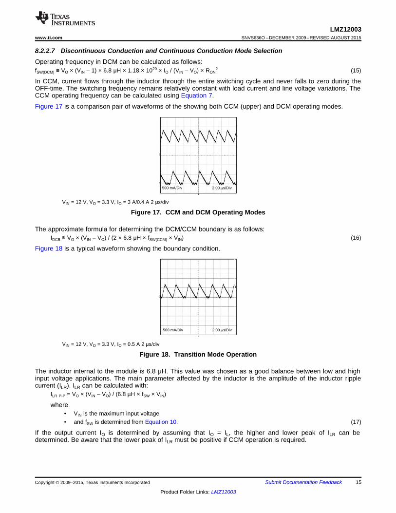
Figure 17 is a comparison pair of waveforms of the showing both CCM (upper) and DCM operating modes.
VIN = 12 V, VO = 3.3 V, IO = 3 A/0.4 A 2 μs/div
Figure 17. CCM and DCM Operating Modes
The approximate formula for determining the DCM/CCM boundary is as follows:IDCB ≊ VO × (VIN – VO) / (2 × 6.8 μH × fSW(CCM) × VIN) (16)
Figure 18 is a typical waveform showing the boundary condition.
VIN = 12 V, VO = 3.3 V, IO = 0.5 A 2 μs/div
Figure 18. Transition Mode Operation
The inductor internal to the module is 6.8 μH. This value was chosen as a good balance between low and highinput voltage applications. The main parameter affected by the inductor is the amplitude of the inductor ripplecurrent (ILR). ILR can be calculated with:
ILR P-P = VO × (VIN – VO) / (6.8 µH × fSW × VIN)
where• VIN is the maximum input voltage• and fSW is determined from Equation 10. (17)
If the output current IO is determined by assuming that IO = IL, the higher and lower peak of ILR can bedetermined. Be aware that the lower peak of ILR must be positive if CCM operation is required.
Copyright © 2009–2015, Texas Instruments Incorporated Submit Documentation Feedback 15
Product Folder Links: LMZ12003
LMZ12003SNVS636O –DECEMBER 2009–REVISED AUGUST 2015 www.ti.com
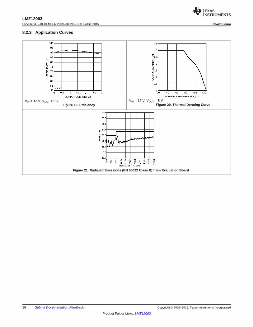
8.2.3 Application Curves
VIN = 12 V, VOUT = 5 VVIN = 12 V, VOUT = 5 VFigure 20. Thermal Derating CurveFigure 19. Efficiency
Figure 21. Radiated Emissions (EN 55022 Class B) from Evaluation Board
16 Submit Documentation Feedback Copyright © 2009–2015, Texas Instruments Incorporated
Product Folder Links: LMZ12003
LMZ12003www.ti.com SNVS636O –DECEMBER 2009–REVISED AUGUST 2015
9 Power Supply RecommendationsThe LMZ12003 device is designed to operate from an input voltage supply range between 4.5 V and 20 V. Thisinput supply should be well regulated and able to withstand maximum input current and maintain a stablevoltage. The resistance of the input supply rail should be low enough that an input current transient does notcause a high enough drop at the LMZ12003 supply voltage that can cause a false UVLO fault triggering andsystem reset. If the input supply is more than a few inches from the LMZ12003, additional bulk capacitance maybe required in addition to the ceramic bypass capacitors. The amount of bulk capacitance is not critical, but a 47-μF or 100-μF electrolytic capacitor is a typical choice.
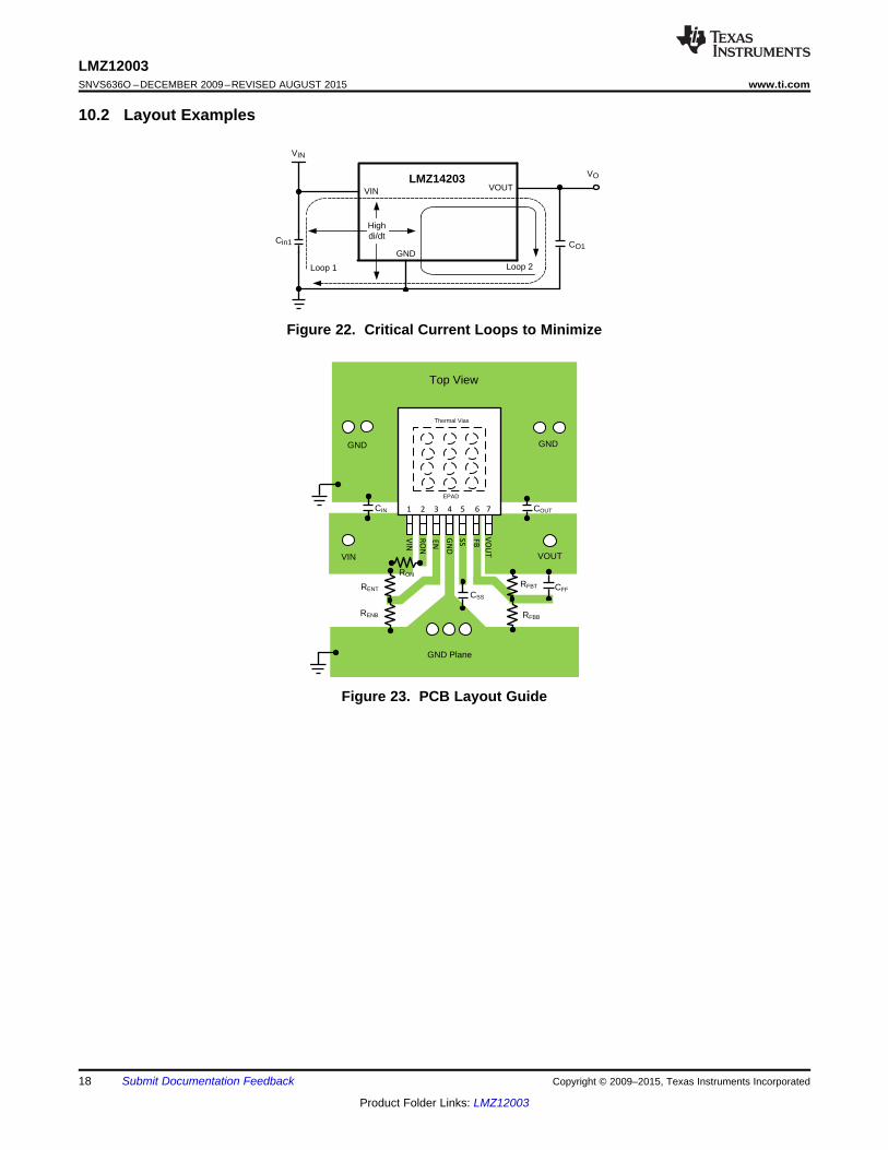
10 Layout
10.1 Layout GuidelinesPCB layout is an important part of DC-DC converter design. Poor board layout can disrupt the performance of aDC-DC converter and surrounding circuitry by contributing to EMI, ground bounce and resistive voltage drop inthe traces. These can send erroneous signals to the DC-DC converter resulting in poor regulation or instability.Good layout can be implemented by following a few simple design rules.1. Minimize area of switched current loops.
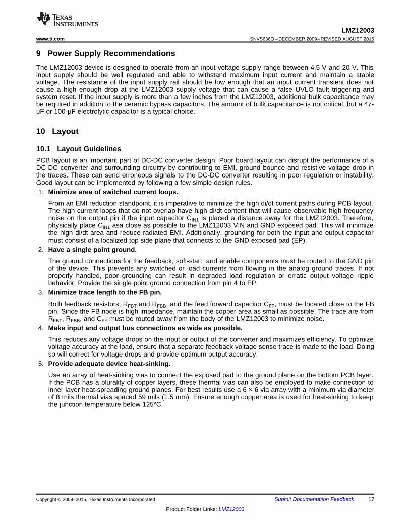
From an EMI reduction standpoint, it is imperative to minimize the high di/dt current paths during PCB layout.The high current loops that do not overlap have high di/dt content that will cause observable high frequencynoise on the output pin if the input capacitor CIN1 is placed a distance away for the LMZ12003. Therefore,physically place CIN1 asa close as possible to the LMZ12003 VIN and GND exposed pad. This will minimizethe high di/dt area and reduce radiated EMI. Additionally, grounding for both the input and output capacitormust consist of a localized top side plane that connects to the GND exposed pad (EP).
2. Have a single point ground.The ground connections for the feedback, soft-start, and enable components must be routed to the GND pinof the device. This prevents any switched or load currents from flowing in the analog ground traces. If notproperly handled, poor grounding can result in degraded load regulation or erratic output voltage ripplebehavior. Provide the single point ground connection from pin 4 to EP.
3. Minimize trace length to the FB pin.Both feedback resistors, RFBT and RFBB, and the feed forward capacitor CFF, must be located close to the FBpin. Since the FB node is high impedance, maintain the copper area as small as possible. The trace are fromRFBT, RFBB, and CFF must be routed away from the body of the LMZ12003 to minimize noise.
4. Make input and output bus connections as wide as possible.This reduces any voltage drops on the input or output of the converter and maximizes efficiency. To optimizevoltage accuracy at the load, ensure that a separate feedback voltage sense trace is made to the load. Doingso will correct for voltage drops and provide optimum output accuracy.
5. Provide adequate device heat-sinking.Use an array of heat-sinking vias to connect the exposed pad to the ground plane on the bottom PCB layer.If the PCB has a plurality of copper layers, these thermal vias can also be employed to make connection toinner layer heat-spreading ground planes. For best results use a 6 × 6 via array with a minimum via diameterof 8 mils thermal vias spaced 59 mils (1.5 mm). Ensure enough copper area is used for heat-sinking to keepthe junction temperature below 125°C.
Copyright © 2009–2015, Texas Instruments Incorporated Submit Documentation Feedback 17
Product Folder Links: LMZ12003
RON
EN
SS
GND
FB
VIN
1 2 3 4 5 6 7
Top View
VIN
COUT
VOUT
RENT
RON
CSS
GND
Thermal Vias
VOUT
CIN
GND
RENB
CFFRFBT
RFBB
GND Plane
EPAD
VIN
GND
VIN
VO
Cin1 CO1
Loop 1 Loop 2
LMZ14203VOUT
High di/dt
LMZ12003SNVS636O –DECEMBER 2009–REVISED AUGUST 2015 www.ti.com
10.2 Layout Examples
Figure 22. Critical Current Loops to Minimize
Figure 23. PCB Layout Guide
18 Submit Documentation Feedback Copyright © 2009–2015, Texas Instruments Incorporated
Product Folder Links: LMZ12003
LMZ12003www.ti.com SNVS636O –DECEMBER 2009–REVISED AUGUST 2015
Layout Examples (continued)
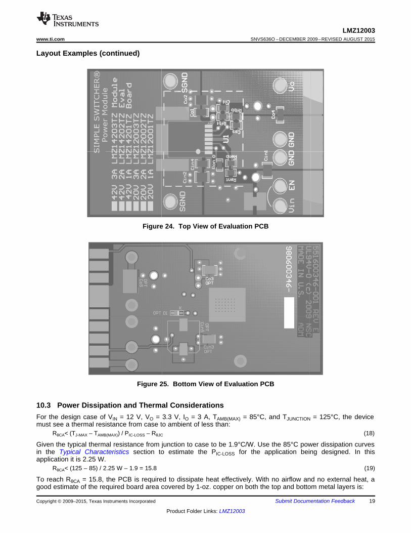
Figure 24. Top View of Evaluation PCB
Figure 25. Bottom View of Evaluation PCB
10.3 Power Dissipation and Thermal ConsiderationsFor the design case of VIN = 12 V, VO = 3.3 V, IO = 3 A, TAMB(MAX) = 85°C, and TJUNCTION = 125°C, the devicemust see a thermal resistance from case to ambient of less than:
RθCA< (TJ-MAX – TAMB(MAX)) / PIC-LOSS – RθJC (18)
Given the typical thermal resistance from junction to case to be 1.9°C/W. Use the 85°C power dissipation curvesin the Typical Characteristics section to estimate the PIC-LOSS for the application being designed. In thisapplication it is 2.25 W.
RθCA< (125 – 85) / 2.25 W – 1.9 = 15.8 (19)
To reach RθCA = 15.8, the PCB is required to dissipate heat effectively. With no airflow and no external heat, agood estimate of the required board area covered by 1-oz. copper on both the top and bottom metal layers is:
Copyright © 2009–2015, Texas Instruments Incorporated Submit Documentation Feedback 19
Product Folder Links: LMZ12003
LMZ12003SNVS636O –DECEMBER 2009–REVISED AUGUST 2015 www.ti.com
Power Dissipation and Thermal Considerations (continued)Board Area_cm2 > 500°C × cm2/W / RθJC (20)
As a result, approximately 31 square cm of 1-oz. copper on top and bottom layers is required for the PCBdesign. The PCB copper heat sink must be connected to the exposed pad. Approximately thirty six, 8 milsthermal vias spaced 59 mils (1.5 mm) apart must connect the top copper to the bottom copper. For an exampleof a high thermal performance PCB layout, refer to the demo board application note AN-2024 SNVA422.
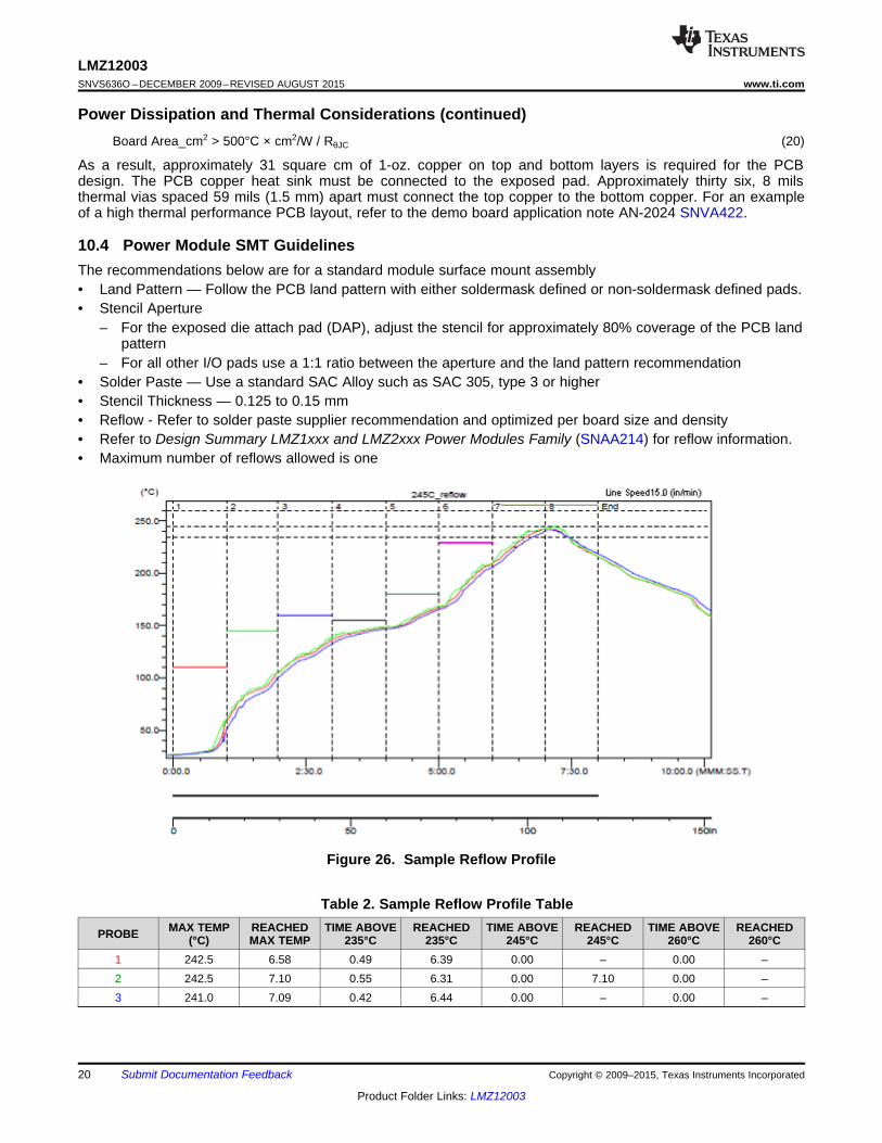
10.4 Power Module SMT GuidelinesThe recommendations below are for a standard module surface mount assembly• Land Pattern — Follow the PCB land pattern with either soldermask defined or non-soldermask defined pads.• Stencil Aperture
– For the exposed die attach pad (DAP), adjust the stencil for approximately 80% coverage of the PCB landpattern
– For all other I/O pads use a 1:1 ratio between the aperture and the land pattern recommendation• Solder Paste — Use a standard SAC Alloy such as SAC 305, type 3 or higher• Stencil Thickness — 0.125 to 0.15 mm• Reflow - Refer to solder paste supplier recommendation and optimized per board size and density• Refer to Design Summary LMZ1xxx and LMZ2xxx Power Modules Family (SNAA214) for reflow information.• Maximum number of reflows allowed is one
Figure 26. Sample Reflow Profile
Table 2. Sample Reflow Profile TableMAX TEMP REACHED TIME ABOVE REACHED TIME ABOVE REACHED TIME ABOVE REACHEDPROBE (°C) MAX TEMP 235°C 235°C 245°C 245°C 260°C 260°C
1 242.5 6.58 0.49 6.39 0.00 – 0.00 –2 242.5 7.10 0.55 6.31 0.00 7.10 0.00 –3 241.0 7.09 0.42 6.44 0.00 – 0.00 –
20 Submit Documentation Feedback Copyright © 2009–2015, Texas Instruments Incorporated
Product Folder Links: LMZ12003
LMZ12003www.ti.com SNVS636O –DECEMBER 2009–REVISED AUGUST 2015
11 Device and Documentation Support
11.1 Device Support
11.1.1 Third-Party Products DisclaimerTI'S PUBLICATION OF INFORMATION REGARDING THIRD-PARTY PRODUCTS OR SERVICES DOES NOTCONSTITUTE AN ENDORSEMENT REGARDING THE SUITABILITY OF SUCH PRODUCTS OR SERVICESOR A WARRANTY, REPRESENTATION OR ENDORSEMENT OF SUCH PRODUCTS OR SERVICES, EITHERALONE OR IN COMBINATION WITH ANY TI PRODUCT OR SERVICE.
11.1.2 Development SupportFor developmental support, see the following:
WEBENCH Tool, http://www.ti.com/webench
11.2 Documentation Support
11.2.1 Related DocumentationFor related documentation, see the following:• AN-2027 Inverting Application for the LMZ14203 SIMPLE SWITCHER Power Module, (SNVA425)• Absolute Maximum Ratings for Soldering, (SNOA549)• AN-2024 LMZ1420x / LMZ1200x Evaluation Board (SNVA422)• AN-2085 LMZ23605/03, LMZ22005/03 Evaluation Board (SNVA457)• AN-2054 Evaluation Board for LM10000 - PowerWise AVS System Controller (SNVA437)• AN-2020 Thermal Design By Insight, Not Hindsight (SNVA419)• AN-2026 Effect of PCB Design on Thermal Performance of SIMPLE SWITCHER Power Modules (SNVA424)• Design Summary LMZ1xxx and LMZ2xxx Power Modules Family (SNAA214)
11.3 Community ResourcesThe following links connect to TI community resources. Linked contents are provided "AS IS" by the respectivecontributors. They do not constitute TI specifications and do not necessarily reflect TI's views; see TI's Terms ofUse.
TI E2E™ Online Community TI's Engineer-to-Engineer (E2E) Community. Created to foster collaborationamong engineers. At e2e.ti.com, you can ask questions, share knowledge, explore ideas and helpsolve problems with fellow engineers.
Design Support TI's Design Support Quickly find helpful E2E forums along with design support tools andcontact information for technical support.
11.4 TrademarksE2E is a trademark of Texas Instruments.WEBENCH, SIMPLE SWITCHER are registered trademarks of Texas Instruments.All other trademarks are the property of their respective owners.
11.5 Electrostatic Discharge CautionThese devices have limited built-in ESD protection. The leads should be shorted together or the device placed in conductive foamduring storage or handling to prevent electrostatic damage to the MOS gates.
11.6 GlossarySLYZ022 — TI Glossary.
This glossary lists and explains terms, acronyms, and definitions.
Copyright © 2009–2015, Texas Instruments Incorporated Submit Documentation Feedback 21
Product Folder Links: LMZ12003

LMZ12003SNVS636O –DECEMBER 2009–REVISED AUGUST 2015 www.ti.com
12 Mechanical, Packaging, and Orderable InformationThe following pages include mechanical, packaging, and orderable information. This information is the mostcurrent data available for the designated devices. This data is subject to change without notice and revision ofthis document. For browser-based versions of this data sheet, refer to the left-hand navigation.
22 Submit Documentation Feedback Copyright © 2009–2015, Texas Instruments Incorporated
Product Folder Links: LMZ12003
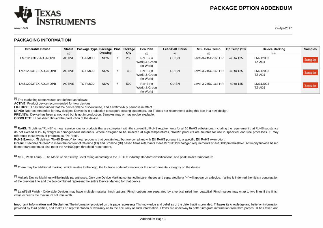
PACKAGE OPTION ADDENDUM
www.ti.com 27-Apr-2017
Addendum-Page 1
PACKAGING INFORMATION
Orderable Device Status(1)
Package Type PackageDrawing
Pins PackageQty
Eco Plan(2)
Lead/Ball Finish(6)
MSL Peak Temp(3)
Op Temp (°C) Device Marking(4/5)
Samples
LMZ12003TZ-ADJ/NOPB ACTIVE TO-PMOD NDW 7 250 RoHS (InWork) & Green
(In Work)
CU SN Level-3-245C-168 HR -40 to 125 LMZ12003TZ-ADJ
LMZ12003TZE-ADJ/NOPB ACTIVE TO-PMOD NDW 7 45 RoHS (InWork) & Green
(In Work)
CU SN Level-3-245C-168 HR -40 to 125 LMZ12003TZ-ADJ
LMZ12003TZX-ADJ/NOPB ACTIVE TO-PMOD NDW 7 500 RoHS (InWork) & Green
(In Work)
CU SN Level-3-245C-168 HR -40 to 125 LMZ12003TZ-ADJ
(1) The marketing status values are defined as follows:ACTIVE: Product device recommended for new designs.LIFEBUY: TI has announced that the device will be discontinued, and a lifetime-buy period is in effect.NRND: Not recommended for new designs. Device is in production to support existing customers, but TI does not recommend using this part in a new design.PREVIEW: Device has been announced but is not in production. Samples may or may not be available.OBSOLETE: TI has discontinued the production of the device.
(2) RoHS: TI defines "RoHS" to mean semiconductor products that are compliant with the current EU RoHS requirements for all 10 RoHS substances, including the requirement that RoHS substancedo not exceed 0.1% by weight in homogeneous materials. Where designed to be soldered at high temperatures, "RoHS" products are suitable for use in specified lead-free processes. TI mayreference these types of products as "Pb-Free".RoHS Exempt: TI defines "RoHS Exempt" to mean products that contain lead but are compliant with EU RoHS pursuant to a specific EU RoHS exemption.Green: TI defines "Green" to mean the content of Chlorine (Cl) and Bromine (Br) based flame retardants meet JS709B low halogen requirements of <=1000ppm threshold. Antimony trioxide basedflame retardants must also meet the <=1000ppm threshold requirement.
(3) MSL, Peak Temp. - The Moisture Sensitivity Level rating according to the JEDEC industry standard classifications, and peak solder temperature.
(4) There may be additional marking, which relates to the logo, the lot trace code information, or the environmental category on the device.
(5) Multiple Device Markings will be inside parentheses. Only one Device Marking contained in parentheses and separated by a "~" will appear on a device. If a line is indented then it is a continuationof the previous line and the two combined represent the entire Device Marking for that device.
(6) Lead/Ball Finish - Orderable Devices may have multiple material finish options. Finish options are separated by a vertical ruled line. Lead/Ball Finish values may wrap to two lines if the finishvalue exceeds the maximum column width.
Important Information and Disclaimer:The information provided on this page represents TI's knowledge and belief as of the date that it is provided. TI bases its knowledge and belief on informationprovided by third parties, and makes no representation or warranty as to the accuracy of such information. Efforts are underway to better integrate information from third parties. TI has taken and
PACKAGE OPTION ADDENDUM
www.ti.com 27-Apr-2017
Addendum-Page 2
continues to take reasonable steps to provide representative and accurate information but may not have conducted destructive testing or chemical analysis on incoming materials and chemicals.TI and TI suppliers consider certain information to be proprietary, and thus CAS numbers and other limited information may not be available for release.
In no event shall TI's liability arising out of such information exceed the total purchase price of the TI part(s) at issue in this document sold by TI to Customer on an annual basis.
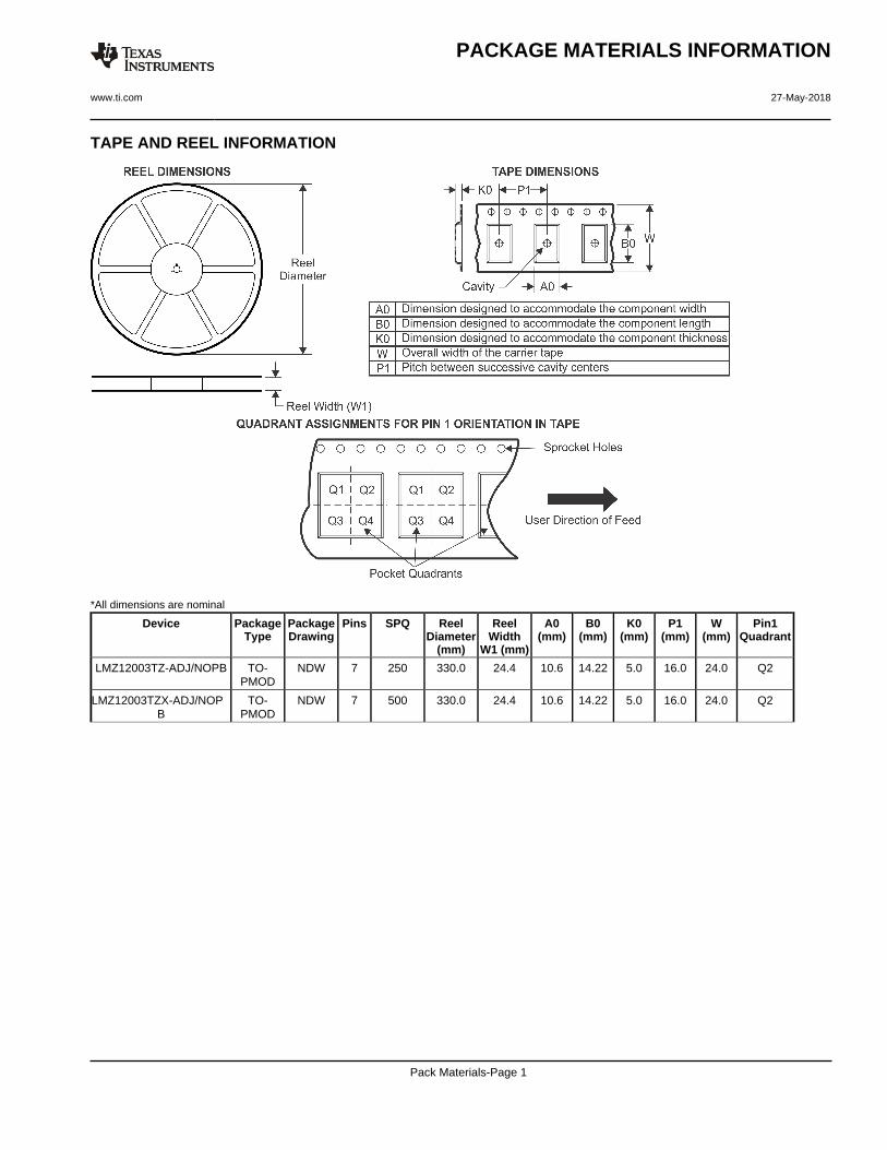
TAPE AND REEL INFORMATION
*All dimensions are nominal
Device PackageType
PackageDrawing
Pins SPQ ReelDiameter
(mm)
ReelWidth
W1 (mm)
A0(mm)
B0(mm)
K0(mm)
P1(mm)
W(mm)
Pin1Quadrant
LMZ12003TZ-ADJ/NOPB TO-PMOD
NDW 7 250 330.0 24.4 10.6 14.22 5.0 16.0 24.0 Q2
LMZ12003TZX-ADJ/NOPB
TO-PMOD
NDW 7 500 330.0 24.4 10.6 14.22 5.0 16.0 24.0 Q2
PACKAGE MATERIALS INFORMATION
www.ti.com 27-May-2018
Pack Materials-Page 1
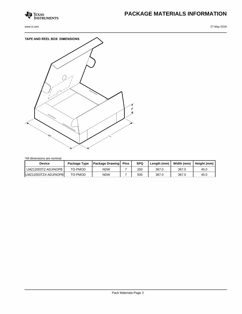
*All dimensions are nominal
Device Package Type Package Drawing Pins SPQ Length (mm) Width (mm) Height (mm)
LMZ12003TZ-ADJ/NOPB TO-PMOD NDW 7 250 367.0 367.0 45.0
LMZ12003TZX-ADJ/NOPB TO-PMOD NDW 7 500 367.0 367.0 45.0
PACKAGE MATERIALS INFORMATION
www.ti.com 27-May-2018
Pack Materials-Page 2
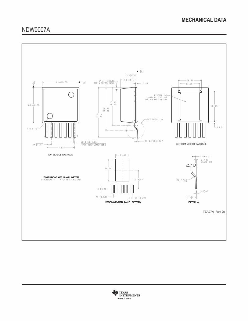
MECHANICAL DATA
NDW0007A
www.ti.com
TZA07A (Rev D)
TOP SIDE OF PACKAGE
BOTTOM SIDE OF PACKAGE
IMPORTANT NOTICE
Texas Instruments Incorporated (TI) reserves the right to make corrections, enhancements, improvements and other changes to itssemiconductor products and services per JESD46, latest issue, and to discontinue any product or service per JESD48, latest issue. Buyersshould obtain the latest relevant information before placing orders and should verify that such information is current and complete.TI’s published terms of sale for semiconductor products (http://www.ti.com/sc/docs/stdterms.htm) apply to the sale of packaged integratedcircuit products that TI has qualified and released to market. Additional terms may apply to the use or sale of other types of TI products andservices.Reproduction of significant portions of TI information in TI data sheets is permissible only if reproduction is without alteration and isaccompanied by all associated warranties, conditions, limitations, and notices. TI is not responsible or liable for such reproduceddocumentation. Information of third parties may be subject to additional restrictions. Resale of TI products or services with statementsdifferent from or beyond the parameters stated by TI for that product or service voids all express and any implied warranties for theassociated TI product or service and is an unfair and deceptive business practice. TI is not responsible or liable for any such statements.Buyers and others who are developing systems that incorporate TI products (collectively, “Designers”) understand and agree that Designersremain responsible for using their independent analysis, evaluation and judgment in designing their applications and that Designers havefull and exclusive responsibility to assure the safety of Designers' applications and compliance of their applications (and of all TI productsused in or for Designers’ applications) with all applicable regulations, laws and other applicable requirements. Designer represents that, withrespect to their applications, Designer has all the necessary expertise to create and implement safeguards that (1) anticipate dangerousconsequences of failures, (2) monitor failures and their consequences, and (3) lessen the likelihood of failures that might cause harm andtake appropriate actions. Designer agrees that prior to using or distributing any applications that include TI products, Designer willthoroughly test such applications and the functionality of such TI products as used in such applications.TI’s provision of technical, application or other design advice, quality characterization, reliability data or other services or information,including, but not limited to, reference designs and materials relating to evaluation modules, (collectively, “TI Resources”) are intended toassist designers who are developing applications that incorporate TI products; by downloading, accessing or using TI Resources in anyway, Designer (individually or, if Designer is acting on behalf of a company, Designer’s company) agrees to use any particular TI Resourcesolely for this purpose and subject to the terms of this Notice.TI’s provision of TI Resources does not expand or otherwise alter TI’s applicable published warranties or warranty disclaimers for TIproducts, and no additional obligations or liabilities arise from TI providing such TI Resources. TI reserves the right to make corrections,enhancements, improvements and other changes to its TI Resources. TI has not conducted any testing other than that specificallydescribed in the published documentation for a particular TI Resource.Designer is authorized to use, copy and modify any individual TI Resource only in connection with the development of applications thatinclude the TI product(s) identified in such TI Resource. NO OTHER LICENSE, EXPRESS OR IMPLIED, BY ESTOPPEL OR OTHERWISETO ANY OTHER TI INTELLECTUAL PROPERTY RIGHT, AND NO LICENSE TO ANY TECHNOLOGY OR INTELLECTUAL PROPERTYRIGHT OF TI OR ANY THIRD PARTY IS GRANTED HEREIN, including but not limited to any patent right, copyright, mask work right, orother intellectual property right relating to any combination, machine, or process in which TI products or services are used. Informationregarding or referencing third-party products or services does not constitute a license to use such products or services, or a warranty orendorsement thereof. Use of TI Resources may require a license from a third party under the patents or other intellectual property of thethird party, or a license from TI under the patents or other intellectual property of TI.TI RESOURCES ARE PROVIDED “AS IS” AND WITH ALL FAULTS. TI DISCLAIMS ALL OTHER WARRANTIES ORREPRESENTATIONS, EXPRESS OR IMPLIED, REGARDING RESOURCES OR USE THEREOF, INCLUDING BUT NOT LIMITED TOACCURACY OR COMPLETENESS, TITLE, ANY EPIDEMIC FAILURE WARRANTY AND ANY IMPLIED WARRANTIES OFMERCHANTABILITY, FITNESS FOR A PARTICULAR PURPOSE, AND NON-INFRINGEMENT OF ANY THIRD PARTY INTELLECTUALPROPERTY RIGHTS. TI SHALL NOT BE LIABLE FOR AND SHALL NOT DEFEND OR INDEMNIFY DESIGNER AGAINST ANY CLAIM,INCLUDING BUT NOT LIMITED TO ANY INFRINGEMENT CLAIM THAT RELATES TO OR IS BASED ON ANY COMBINATION OFPRODUCTS EVEN IF DESCRIBED IN TI RESOURCES OR OTHERWISE. IN NO EVENT SHALL TI BE LIABLE FOR ANY ACTUAL,DIRECT, SPECIAL, COLLATERAL, INDIRECT, PUNITIVE, INCIDENTAL, CONSEQUENTIAL OR EXEMPLARY DAMAGES INCONNECTION WITH OR ARISING OUT OF TI RESOURCES OR USE THEREOF, AND REGARDLESS OF WHETHER TI HAS BEENADVISED OF THE POSSIBILITY OF SUCH DAMAGES.Unless TI has explicitly designated an individual product as meeting the requirements of a particular industry standard (e.g., ISO/TS 16949and ISO 26262), TI is not responsible for any failure to meet such industry standard requirements.Where TI specifically promotes products as facilitating functional safety or as compliant with industry functional safety standards, suchproducts are intended to help enable customers to design and create their own applications that meet applicable functional safety standardsand requirements. Using products in an application does not by itself establish any safety features in the application. Designers mustensure compliance with safety-related requirements and standards applicable to their applications. Designer may not use any TI products inlife-critical medical equipment unless authorized officers of the parties have executed a special contract specifically governing such use.Life-critical medical equipment is medical equipment where failure of such equipment would cause serious bodily injury or death (e.g., lifesupport, pacemakers, defibrillators, heart pumps, neurostimulators, and implantables). Such equipment includes, without limitation, allmedical devices identified by the U.S. Food and Drug Administration as Class III devices and equivalent classifications outside the U.S.TI may expressly designate certain products as completing a particular qualification (e.g., Q100, Military Grade, or Enhanced Product).Designers agree that it has the necessary expertise to select the product with the appropriate qualification designation for their applicationsand that proper product selection is at Designers’ own risk. Designers are solely responsible for compliance with all legal and regulatoryrequirements in connection with such selection.Designer will fully indemnify TI and its representatives against any damages, costs, losses, and/or liabilities arising out of Designer’s non-compliance with the terms and provisions of this Notice.
Mailing Address: Texas Instruments, Post Office Box 655303, Dallas, Texas 75265Copyright © 2018, Texas Instruments Incorporated