0.5 mm 72 mhz cortex-m0+ based microcontroller 8 x 8 x 0 ... · 0.5 mm nxp semiconductors...
TRANSCRIPT
Kinetis KL28Zxxx with 512 KBFlash and 128 KB SRAM72 MHz Cortex-M0+ based Microcontroller
Supports ultra low power ARM based microcontroller withcrystal-less USB feature, large flash and RAM, evolutionary low-power peripherals and security features. This is an ideal solutionfor Sensor Hub applications, Bluetooth, Wi-Fi connectivity, SmartEnergy, Internet of Things, and Edge and Concentrator. Thisdevice offers:
• 128KB SRAM for data processing and connectivity stack• Ultra low dynamic and static power consumption with smart
peripherals for low power applications• Advanced LPI2C and LPSPI supporting asynchronous
DMA master data transition• FlexIO for flexible and high performance interfaces• Crypto acceleration with AES/DES/3DES/MD5/SHA and TRNG• USB FS 2.0 device operation without need of external crystal
Core• ARM® Cortex®-M0+ cores up to 72 MHz in Normal
mode and 96 MHz in High Speed mode
Memories• Up to 512 KB program flash memory• 128 KB SRAM• 32 KB ROM with built-in bootloader
System peripherals• 8-channel DMA controller• Independent clocked Watchdog• Low-leakage wakeup unit• SWD debug interface and Micro Trace Buffer• Bit Manipulation Engine• Memory Mapped Divide and Square Root module
(MMDDVSQ)• Cyclic Redundancy Check (CRC) module• Nested Vector Interrupt Controller (NVIC) supports 32
interrupt vectors• Additional peripheral interrupt support via Interrupt
Multiplexer (INTMUX)
Clocks• System Clock Generator module that includes the
following clock sources:• 48 to 60 MHz high accuracy fast internal
reference clock (FIRC)
Communication interfaces• Three 16-bit Low Power Serial Peripheral Interface
(LPSPI) modules• One EMVSIM module supporting EMV version 4.3,
ISO7816• Three LPUART modules• Three LPI2C modules supporting up to 5 Mbit/s• One SAI module supporting I2S• One FlexIO module emulating UART, SPI, I2S,
camera interface, and Motorola 68K/Intel 8080 bus• USB FS 2.0 device operation without need of
external crystal
Analog Modules
• 16-bit, 24-channel SAR ADC with internal voltagereference
• Two High-speed analog comparators eachcontaining a 6-bit DAC and programmable referenceinput
• One 12-bit DAC• 1.2 V and 2.1 V voltage references (Vref)
Timers• One 6-channel Timer/PWM module• Two 2-channel Timer/PWM modules• Two low-power timers• Two periodic interrupt timers
MKL28Z512Vxx7
121 XFBGA8 x 8 x 0.43 mm Pitch
0.65 mm
100 LQFP14 x 14 x 1.4 mm Pitch
0.5 mm
NXP Semiconductors MKL28Z512Vxx7Data Sheet: Technical Data Rev. 2.1, 06/2016
NXP reserves the right to change the production detail specifications as may berequired to permit improvements in the design of its products.
• 32–40 kHz, or 3–32 MHz crystal oscillator• 1 kHz LPO clock• 8/2 MHz slow internal reference clock (SIRC)• Peripheral Clock Control (PCC) module that
supports asynchronous clocking and clock divideoptions for peripherals.
Human-machine interface• General-purpose input/output up to 97• Low-power hardware touch sensor interface (TSI)
• Secure Real time clock• 56-bit software time stamp timer at 1 MHz
Security and integrity modules• 80-bit unique identification number per chip• MMCAU supports acceleration of the DES, 3DES,
AES, MD5, SHA-1, and SHA-256 algorithms• True Random Number Generator (TRNG)
Operating Characteristics
• Voltage range: 1.71 to 3.6 V• Temperature range: –40 to 105 °C
NOTEThe 121-pin packages for this product is not yet available. However, it is included in aPackage Your Way program for Kinetis MCUs. Visit nxp.com/KPYW for moredetails.
Ordering Information 1
Part Number Memory Package IO and ADC channels
Flash (KB) SRAM (KB) Pin count Package GPIOs GPIOs(INT/HD)
ADCchannels(SE/DP)
MKL28Z512VLL7
512 128 100 LQFP 82 82/8 27/4
MKL28Z512VDC72
512 128 121 XFBGA 97 97/8 27/4
1. To confirm current availability of ordererable part numbers, go to http://www.nxp.com and perform a part number search.2. Package Your Way.
Related Resources
Type Description Resource
SelectorGuide
The NXP Solution Advisor is a web-based tool that features interactiveapplication wizards and a dynamic product selector.
Solution Advisor
Product Brief The Product Brief contains concise overview/summary information toenable quick evaluation of a device for design suitability.
KL2XPB1
ReferenceManual
The Reference Manual contains a comprehensive description of thestructure and function (operation) of a device.
MKL28ZRM1
Data Sheet The Data Sheet includes electrical characteristics and signalconnections.
MKL28Z512Vxx71
Chip Errata The chip mask set Errata provides additional or corrective information fora particular device mask set.
KINETIS_L_1N52N1
Packagedrawing
Package dimensions are provided in package drawings. • 121-XFBGA:98ASA00595D1
• 100-LQFP:98ASS23308W1
1. To find the associated resource, go to http://www.nxp.com and perform a search using this term.
2 Kinetis KL28Zxxx with 512 KB Flash and 128 KB SRAM, Rev. 2.1, 06/2016
NXP Semiconductors

INTM
UX0
GPIO
TSI
I2C
Audio
UARTSPIWDOGResetTimerTimerTimer
Clocks/Oscillators
Cortex-M0+Platform
CTI
Core
DMARequests
DMAMux0 •••
SystemInterrupts
IO Port
SWD
ADCInputs
DACOutputs
ReferenceInputs
Port D
Port A
Port B
Port C
EMVSIM
VREFDAC0 LPO1KPLL
CMP0
XTALOSC
ANALOG SCG
SIRCFIRCTempMonitorADC0
CMP1
SWD-DP
MCM
CAU
DVSQ
MTB
DWT
FlexIO8/16-bit
Parallel I/F
PortD
EMVSIM
PortC
PortB
PortA
SRAM128KB
ROM32KB
FTFANVICSYSTICK
Cortex-M0+
MPUDBG AWIC
Core Memory-Mapped Module
Other Module suchas test/analog
Bus Components Platform Domain
Analog DomainMemory protectionGaskets
DAP
secexsc
S
CM0+ Platform
AHB32
AIPS0 IPBUS
AIPS1 IPBUS
LEGEND:
DMA08-channel
AIPS0
FLASH 1256KB
FLASH 0256KBFMC
BMEAIPS1
MDM-AP AHB-AP0
s2
m1
m0
s1
s0
m2
s3
AXBS
1xUSB
Port EPortE
USB0
M0+ DBG
TPM2
LPUART2PMC CRC LPTMR
1LPTMR
0LPSPI
2WDOG
0
SCG SRTC LPIT0 SIMLLWURCM
RGPIO
SAI0
LPI2C2
TSI0
I2C
UART
SPI
Timer TPM0/1
LPSPI0/1
LPUART0/1
LPI2C0/1
FlexIO0
Reference
Synchronizer
TRNG
MSCM
USB SRAM
CTI
SR
AM
+P
PB
CTR
L
USB
USBVREG
0
TSTMR
Timer
AHB
BME
0
PCC
PCC
TRGMUX
TRGMUX
mux
SMC
Figure 1. KL28Z block diagram
Kinetis KL28Zxxx with 512 KB Flash and 128 KB SRAM, Rev. 2.1, 06/2016 3
NXP Semiconductors
Table of Contents
1 Ratings.................................................................................. 5
1.1 Thermal handling ratings............................................... 5
1.2 Moisture handling ratings...............................................5
1.3 ESD handling ratings..................................................... 5
1.4 Voltage and current operating ratings............................5
2 General................................................................................. 6
2.1 AC electrical characteristics...........................................6
2.2 Nonswitching electrical specifications............................7
2.2.1 Voltage and current operating requirements..... 7
2.2.2 LVD, HVD, and POR operating requirements... 7
2.2.3 Voltage and current operating behaviors...........8
2.2.4 Power mode transition operating behaviors...... 9
2.2.5 Power consumption operating behaviors.......... 10
2.2.6 EMC radiated emissions operating behaviors... 19
2.2.7 Designing with radiated emissions in mind........20
2.2.8 Capacitance attributes.......................................20
2.3 Switching specifications.................................................20
2.3.1 Device clock specifications................................20
2.3.2 General switching specifications....................... 21
2.4 Thermal specifications................................................... 23
2.4.1 Thermal operating requirements....................... 23
2.4.2 Thermal attributes..............................................23
3 Peripheral operating requirements and behaviors................ 24
3.1 Core modules................................................................ 24
3.1.1 SWD electricals ................................................ 24
3.2 System modules............................................................ 26
3.3 Clock modules............................................................... 26
3.3.1 System Clock Generation (SCG) specifications 26
3.3.2 Oscillator electrical specifications......................28
3.4 Memories and memory interfaces................................. 30
3.4.1 Flash electrical specifications............................ 30
3.5 Security and integrity modules.......................................32
3.6 Analog............................................................................32
3.6.1 ADC electrical specifications............................. 32
3.6.2 Voltage reference electrical specifications........ 36
3.6.3 CMP and 6-bit DAC electrical specifications..... 38
3.6.4 12-bit DAC electrical characteristics..................40
3.7 Timers............................................................................43
3.8 Communication interfaces............................................. 43
3.8.1 EMV SIM specifications.....................................43
3.8.2 USB electrical specifications............................. 48
3.8.3 USB VREG electrical specifications.................. 49
3.8.4 LPSPI switching specifications.......................... 49
3.8.5 LPI2C.................................................................54
3.8.6 LPUART............................................................ 54
3.8.7 I2S/SAI switching specifications........................ 55
3.9 Human-machine interfaces (HMI)..................................59
3.9.1 TSI electrical specifications............................... 59
4 Dimensions........................................................................... 59
4.1 Obtaining package dimensions......................................59
5 Pinouts and Packaging......................................................... 60
5.1 KL28Z Signal Multiplexing and Pin Assignments.......... 60
5.2 KL28Z Pinouts............................................................... 65
6 Ordering parts....................................................................... 67
6.1 Determining valid orderable parts..................................67
7 Design considerations...........................................................68
7.1 Hardware design considerations................................... 68
7.1.1 Printed circuit board recommendations............. 68
7.1.2 Power delivery system.......................................68
7.1.3 Analog design....................................................69
7.1.4 Digital design..................................................... 70
7.1.5 Crystal oscillator................................................ 74
7.2 Software considerations................................................ 75
8 Part identification...................................................................76
8.1 Description.....................................................................76
8.2 Format........................................................................... 76
8.3 Fields............................................................................. 76
8.4 Example.........................................................................77
9 Terminology and guidelines.................................................. 77
9.1 Definitions...................................................................... 77
9.2 Examples....................................................................... 78
9.3 Typical-value conditions................................................ 78
9.4 Relationship between ratings and operating
requirements..................................................................79
9.5 Guidelines for ratings and operating requirements........79
10 Revision History.................................................................... 80
4 Kinetis KL28Zxxx with 512 KB Flash and 128 KB SRAM, Rev. 2.1, 06/2016
NXP Semiconductors

1 Ratings
1.1 Thermal handling ratingsTable 1. Thermal handling ratings
Symbol Description Min. Max. Unit Notes
TSTG Storage temperature –55 150 °C 1
TSDR Solder temperature, lead-free — 260 °C 2
1. Determined according to JEDEC Standard JESD22-A103, High Temperature Storage Life.2. Determined according to IPC/JEDEC Standard J-STD-020, Moisture/Reflow Sensitivity Classification for Nonhermetic
Solid State Surface Mount Devices.
1.2 Moisture handling ratingsTable 2. Moisture handling ratings
Symbol Description Min. Max. Unit Notes
MSL Moisture sensitivity level — 3 — 1
1. Determined according to IPC/JEDEC Standard J-STD-020, Moisture/Reflow Sensitivity Classification for NonhermeticSolid State Surface Mount Devices.
1.3 ESD handling ratingsTable 3. ESD handling ratings
Symbol Description Min. Max. Unit Notes
VHBM Electrostatic discharge voltage, human body model –2000 +2000 V 1
VCDM Electrostatic discharge voltage, charged-devicemodel
–500 +500 V 2
ILAT Latch-up current at ambient temperature of 105 °C –100 +100 mA 3
1. Determined according to JEDEC Standard JESD22-A114, Electrostatic Discharge (ESD) Sensitivity Testing HumanBody Model (HBM).
2. Determined according to JEDEC Standard JESD22-C101, Field-Induced Charged-Device Model Test Method forElectrostatic-Discharge-Withstand Thresholds of Microelectronic Components.
3. Determined according to JEDEC Standard JESD78, IC Latch-Up Test.
Ratings
Kinetis KL28Zxxx with 512 KB Flash and 128 KB SRAM, Rev. 2.1, 06/2016 5
NXP Semiconductors
1.4 Voltage and current operating ratingsTable 4. Voltage and current operating ratings
Symbol Description Min. Max. Unit
VDD Digital supply voltage –0.3 3.8 V
IDD Digital supply current — 120 mA
VIO IO pin input voltage –0.3 VDD + 0.3 V
ID Instantaneous maximum current single pin limit (applies toall port pins)
–25 25 mA
VDDA Analog supply voltage VDD – 0.3 VDD + 0.3 V
VUSB_DP USB_DP input voltage –0.3 3.63 V
VUSB_DM USB_DM input voltage –0.3 3.63 V
VREGIN USB regulator input –0.3 6.0 V
2 General
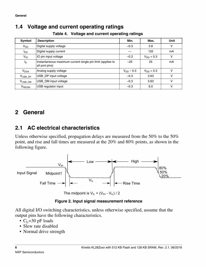
2.1 AC electrical characteristics
Unless otherwise specified, propagation delays are measured from the 50% to the 50%point, and rise and fall times are measured at the 20% and 80% points, as shown in thefollowing figure.
80%
20%50%
VIL
Input Signal
VIH
Fall Time
HighLow
Rise Time
Midpoint1
The midpoint is VIL + (VIH - VIL) / 2
Figure 2. Input signal measurement reference
All digital I/O switching characteristics, unless otherwise specified, assume that theoutput pins have the following characteristics.
• CL=30 pF loads• Slew rate disabled• Normal drive strength
General
6 Kinetis KL28Zxxx with 512 KB Flash and 128 KB SRAM, Rev. 2.1, 06/2016
NXP Semiconductors
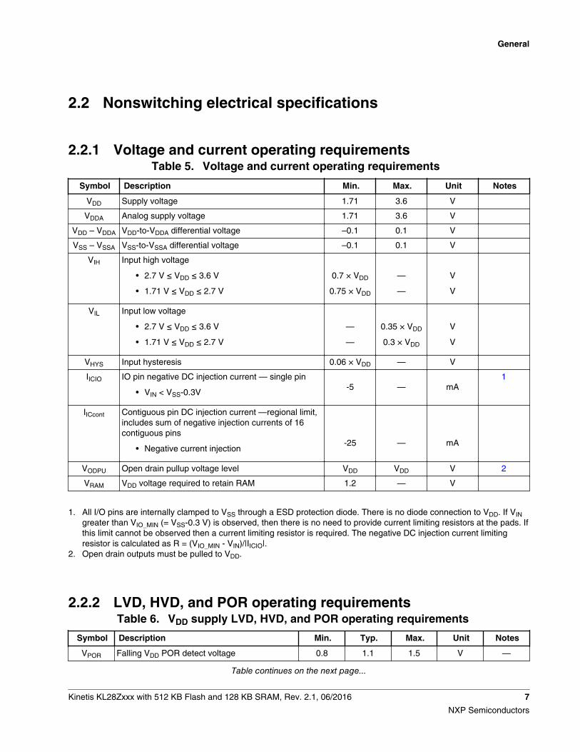
2.2 Nonswitching electrical specifications
2.2.1 Voltage and current operating requirementsTable 5. Voltage and current operating requirements
Symbol Description Min. Max. Unit Notes
VDD Supply voltage 1.71 3.6 V
VDDA Analog supply voltage 1.71 3.6 V
VDD – VDDA VDD-to-VDDA differential voltage –0.1 0.1 V
VSS – VSSA VSS-to-VSSA differential voltage –0.1 0.1 V
VIH Input high voltage
• 2.7 V ≤ VDD ≤ 3.6 V
• 1.71 V ≤ VDD ≤ 2.7 V
0.7 × VDD
0.75 × VDD
—
—
V
V
VIL Input low voltage
• 2.7 V ≤ VDD ≤ 3.6 V
• 1.71 V ≤ VDD ≤ 2.7 V
—
—
0.35 × VDD
0.3 × VDD
V
V
VHYS Input hysteresis 0.06 × VDD — V
IICIO IO pin negative DC injection current — single pin
• VIN < VSS-0.3V-5 — mA
1
IICcont Contiguous pin DC injection current —regional limit,includes sum of negative injection currents of 16contiguous pins
• Negative current injection-25 — mA
VODPU Open drain pullup voltage level VDD VDD V 2
VRAM VDD voltage required to retain RAM 1.2 — V
1. All I/O pins are internally clamped to VSS through a ESD protection diode. There is no diode connection to VDD. If VINgreater than VIO_MIN (= VSS-0.3 V) is observed, then there is no need to provide current limiting resistors at the pads. Ifthis limit cannot be observed then a current limiting resistor is required. The negative DC injection current limitingresistor is calculated as R = (VIO_MIN - VIN)/|IICIO|.
2. Open drain outputs must be pulled to VDD.
2.2.2 LVD, HVD, and POR operating requirementsTable 6. VDD supply LVD, HVD, and POR operating requirements
Symbol Description Min. Typ. Max. Unit Notes
VPOR Falling VDD POR detect voltage 0.8 1.1 1.5 V —
Table continues on the next page...
General
Kinetis KL28Zxxx with 512 KB Flash and 128 KB SRAM, Rev. 2.1, 06/2016 7
NXP Semiconductors
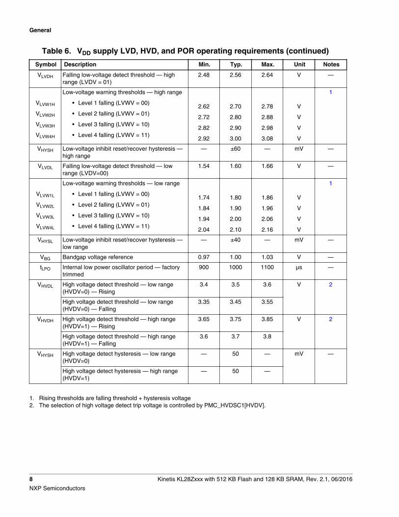
Table 6. VDD supply LVD, HVD, and POR operating requirements (continued)
Symbol Description Min. Typ. Max. Unit Notes
VLVDH Falling low-voltage detect threshold — highrange (LVDV = 01)
2.48 2.56 2.64 V —
VLVW1H
VLVW2H
VLVW3H
VLVW4H
Low-voltage warning thresholds — high range
• Level 1 falling (LVWV = 00)
• Level 2 falling (LVWV = 01)
• Level 3 falling (LVWV = 10)
• Level 4 falling (LVWV = 11)
2.62
2.72
2.82
2.92
2.70
2.80
2.90
3.00
2.78
2.88
2.98
3.08
V
V
V
V
1
VHYSH Low-voltage inhibit reset/recover hysteresis —high range
— ±60 — mV —
VLVDL Falling low-voltage detect threshold — lowrange (LVDV=00)
1.54 1.60 1.66 V —
VLVW1L
VLVW2L
VLVW3L
VLVW4L
Low-voltage warning thresholds — low range
• Level 1 falling (LVWV = 00)
• Level 2 falling (LVWV = 01)
• Level 3 falling (LVWV = 10)
• Level 4 falling (LVWV = 11)
1.74
1.84
1.94
2.04
1.80
1.90
2.00
2.10
1.86
1.96
2.06
2.16
V
V
V
V
1
VHYSL Low-voltage inhibit reset/recover hysteresis —low range
— ±40 — mV —
VBG Bandgap voltage reference 0.97 1.00 1.03 V —
tLPO Internal low power oscillator period — factorytrimmed
900 1000 1100 μs —
VHVDL High voltage detect threshold — low range(HVDV=0) — Rising
3.4 3.5 3.6 V 2
High voltage detect threshold — low range(HVDV=0) — Falling
3.35 3.45 3.55
VHVDH High voltage detect threshold — high range(HVDV=1) — Rising
3.65 3.75 3.85 V 2
High voltage detect threshold — high range(HVDV=1) — Falling
3.6 3.7 3.8
VHYSH High voltage detect hysteresis — low range(HVDV=0)
— 50 — mV —
High voltage detect hysteresis — high range(HVDV=1)
— 50 —
1. Rising thresholds are falling threshold + hysteresis voltage2. The selection of high voltage detect trip voltage is controlled by PMC_HVDSC1[HVDV].
General
8 Kinetis KL28Zxxx with 512 KB Flash and 128 KB SRAM, Rev. 2.1, 06/2016
NXP Semiconductors
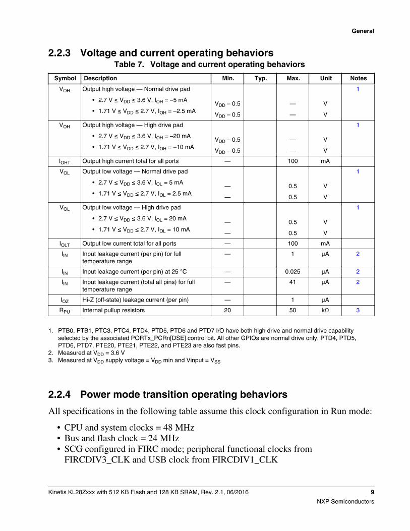
2.2.3 Voltage and current operating behaviorsTable 7. Voltage and current operating behaviors
Symbol Description Min. Typ. Max. Unit Notes
VOH Output high voltage — Normal drive pad
• 2.7 V ≤ VDD ≤ 3.6 V, IOH = –5 mA
• 1.71 V ≤ VDD ≤ 2.7 V, IOH = –2.5 mA
VDD – 0.5
VDD – 0.5
—
—
V
V
1
VOH Output high voltage — High drive pad
• 2.7 V ≤ VDD ≤ 3.6 V, IOH = –20 mA
• 1.71 V ≤ VDD ≤ 2.7 V, IOH = –10 mA
VDD – 0.5
VDD – 0.5
—
—
V
V
1
IOHT Output high current total for all ports — 100 mA
VOL Output low voltage — Normal drive pad
• 2.7 V ≤ VDD ≤ 3.6 V, IOL = 5 mA
• 1.71 V ≤ VDD ≤ 2.7 V, IOL = 2.5 mA
—
—
0.5
0.5
V
V
1
VOL Output low voltage — High drive pad
• 2.7 V ≤ VDD ≤ 3.6 V, IOL = 20 mA
• 1.71 V ≤ VDD ≤ 2.7 V, IOL = 10 mA
—
—
0.5
0.5
V
V
1
IOLT Output low current total for all ports — 100 mA
IIN Input leakage current (per pin) for fulltemperature range
— 1 μA 2
IIN Input leakage current (per pin) at 25 °C — 0.025 μA 2
IIN Input leakage current (total all pins) for fulltemperature range
— 41 μA 2
IOZ Hi-Z (off-state) leakage current (per pin) — 1 μA
RPU Internal pullup resistors 20 50 kΩ 3
1. PTB0, PTB1, PTC3, PTC4, PTD4, PTD5, PTD6 and PTD7 I/O have both high drive and normal drive capabilityselected by the associated PORTx_PCRn[DSE] control bit. All other GPIOs are normal drive only. PTD4, PTD5,PTD6, PTD7, PTE20, PTE21, PTE22, and PTE23 are also fast pins.
2. Measured at VDD = 3.6 V3. Measured at VDD supply voltage = VDD min and Vinput = VSS
2.2.4 Power mode transition operating behaviors
All specifications in the following table assume this clock configuration in Run mode:
• CPU and system clocks = 48 MHz• Bus and flash clock = 24 MHz• SCG configured in FIRC mode; peripheral functional clocks from
FIRCDIV3_CLK and USB clock from FIRCDIV1_CLK
General
Kinetis KL28Zxxx with 512 KB Flash and 128 KB SRAM, Rev. 2.1, 06/2016 9
NXP Semiconductors
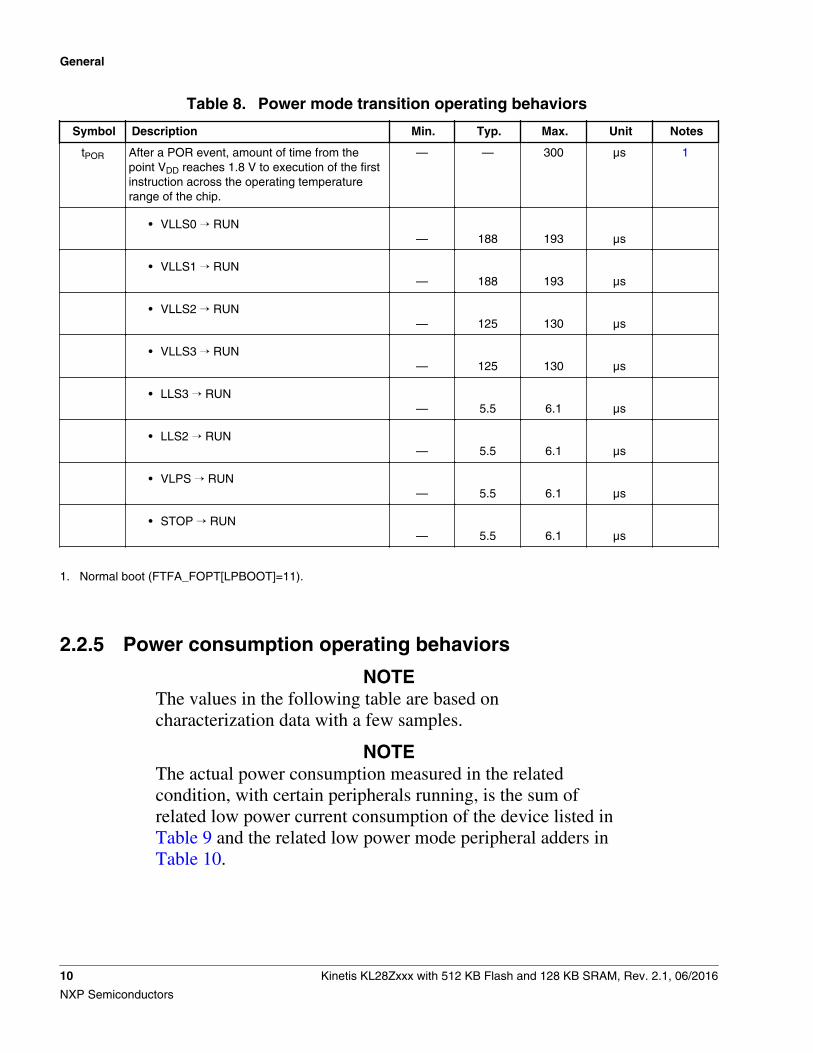
Table 8. Power mode transition operating behaviors
Symbol Description Min. Typ. Max. Unit Notes
tPOR After a POR event, amount of time from thepoint VDD reaches 1.8 V to execution of the firstinstruction across the operating temperaturerange of the chip.
— — 300 μs 1
• VLLS0 → RUN
—
188
193
μs
• VLLS1 → RUN
—
188
193
μs
• VLLS2 → RUN
—
125
130
μs
• VLLS3 → RUN
—
125
130
μs
• LLS3 → RUN
—
5.5
6.1
μs
• LLS2 → RUN
—
5.5
6.1
μs
• VLPS → RUN
—
5.5
6.1
μs
• STOP → RUN
—
5.5
6.1
μs
1. Normal boot (FTFA_FOPT[LPBOOT]=11).
2.2.5 Power consumption operating behaviors
NOTEThe values in the following table are based oncharacterization data with a few samples.
NOTEThe actual power consumption measured in the relatedcondition, with certain peripherals running, is the sum ofrelated low power current consumption of the device listed inTable 9 and the related low power mode peripheral adders inTable 10.
General
10 Kinetis KL28Zxxx with 512 KB Flash and 128 KB SRAM, Rev. 2.1, 06/2016
NXP Semiconductors
NOTEThe maximum values represent characterized resultsequivalent to the mean plus three times the standarddeviation (mean + 3σ).
Table 9. Power consumption operating behaviors
Symbol Description Min. Typ. Max. Unit Notes
IDDA Analog supply current — — See note mA 1
IDD_HSRUN High speed run mode current at 96MHz - all peripheral clocks disabled,code executing from flash, while(1)loop
• at 1.8 V
• at 3.0 V
—
—
12.6
12.8
17.4
17.6
mA
mA
2
IDD_HSRUN High speed run mode current at 96MHz - all peripheral clocks enabled,code executing from flash, while(1)loop
• at 1.8 V
• at 3.0 V
—
—
15.5
15.7
20.4
20.6
mA
mA
3
IDD_RUN Run mode current at 72 MHz - allperipheral clocks disabled, codeexecuting from flash, while(1) loop
• at 1.8 V
• at 3.0 V—
—
9.4
9.6
13.6
13.8
mA
mA
4
IDD_RUN Run mode current at 48 Mhz - allperipheral clocks disabled, codeexecuting from flash, while(1) loop
• at 1.8 V
• at 3.0 V
—
—
7.3
7.4
11.4
11.5
mA
mA
5
IDD_RUN Run mode current at 72 MHz - allperipheral clocks enabled, codeexecuting from flash, while(1) loop
• at 1.8 V
• at 3.0 V
—
—
11.6
11.7
15.9
16.0
mA
mA
6
IDD_RUN Run mode current at 48 Mhz - allperipheral clocks enabled, codeexecuting from flash, while(1) loop
• at 1.8 V
• at 3.0 V
—
—
8.9
9.1
13.1
13.3
mA
mA
7
Table continues on the next page...
General
Kinetis KL28Zxxx with 512 KB Flash and 128 KB SRAM, Rev. 2.1, 06/2016 11
NXP Semiconductors
Table 9. Power consumption operating behaviors (continued)
Symbol Description Min. Typ. Max. Unit Notes
IDD_WAIT Wait mode high frequency current at 72MHz, at 3.0 V - all peripheral clocksdisabled, while(1) loop
— 7.0 9.0 mA 4
IDD_WAIT Wait mode current at 3.0 V at 48 Mhz— all peripheral clocks disabled,while(1) loop
— 5.7 10.4 mA 5
IDD_VLPR Very-low-power run mode current at3.0 V — all peripheral clocks enabledat 4 MHz, while(1) loop
— 483.7 1011.7 μA 8
IDD_VLPR Very-low-power run mode current at3.0 V — all peripheral clocks enabledat 8 MHz, while(1) loop
— 557.6 1720.2 μA 9
IDD_VLPR Very-low-power run mode current at3.0 V — all peripheral clocks disabledat 4 MHz, while(1) loop
— 400.3 926.5 μA 10
IDD_VLPR Very-low-power run mode current at3.0 V — all peripheral clocks disabledat 8 MHz, while(1) loop
— 415.2 941.1 μA 11
IDD_VLPW Very-low-power wait mode current at3.0 V — all peripheral clocks disabledat 4 MHz, while(1) loop
— 285.9 1145.6 μA 10
IDD_VLPW Very-low-power wait mode current at3.0 V — all peripheral clocks disabledat 8 MHz, while(1) loop
— 415.6 1498.7 μA 11
IDD_STOP Stop mode current at 3.0 V• -40 to 25 °C
• at 50 °C
• at 70 °C
• at 85 °C
• at 105 °C
—
—
—
—
—
264.5
287.0
325.3
374.7
496.7
320.5
356.1
445.4
590.8
952.3
μA
IDD_VLPS Very-low-power stop mode current at3.0 V
• -40 to 25 °C
• at 50 °C
• at 70 °C
• at 85 °C
• at 105 °C
—
—
—
—
—
4.2
11.0
24.0
44.0
93.4
16.4
35.9
84.5
156.2
300.2
μA
IDD_LLS2 Low-leakage stop mode 2 current at3.0 V
• -40 to 25 °C
• at 50 °C
• at 70 °C
—
—
—
—
2.7
4.7
8.6
14.7
5.4
10.6
22.7
49.0
μA
Table continues on the next page...
General
12 Kinetis KL28Zxxx with 512 KB Flash and 128 KB SRAM, Rev. 2.1, 06/2016
NXP Semiconductors
Table 9. Power consumption operating behaviors (continued)
Symbol Description Min. Typ. Max. Unit Notes
• at 85 °C
• at 105 °C
— 30.4 88.6
IDD_LLS3 Low-leakage stop mode 3 current at3.0 V
• -40 to 25 °C
• at 50 °C
• at 70 °C
• at 85 °C
• at 105 °C
—
—
—
—
—
3.0
5.9
11.4
19.7
40.9
5.9
14.5
32.0
65.2
122.0
μA
IDD_VLLS3 Very-low-leakage stop mode 3 currentat 3.0 V
• -40 to 25 °C
• at 50 °C
• at 70 °C
• at 85 °C
• at 105 °C
—
—
—
—
—
2.2
4.6
9.0
15.9
33.1
5.1
10.9
24.4
44.8
91.0
μA
IDD_VLLS2 Very-low-leakage stop mode 2 currentat 3.0 V
• -40 to 25 °C
• at 50 °C
• at 70 °C
• at 85 °C
• at 105 °C
—
—
—
—
—
1.8
3.3
6.1
10.4
21.6
3.4
6.8
14.5
26.4
54.4
μA
IDD_VLLS1 Very-low-leakage stop mode 1 currentat 3.0V
• -40 to 25 °C
• at 50 °C
• at 70 °C
• at 85 °C
• at 105 °C
—
—
—
—
—
0.65
1.1
2.1
3.6
8.5
0.88
1.6
3.3
21.0
32.2
μA
IDD_VLLS0 Very-low-leakage stop mode 0 current(SMC_STOPCTRL[PORPO] = 0) at 3.0V
• -40 to 25 °C
• at 50 °C
• at 70 °C
—
—
—
—
—
372.0
768.6
1734
3291
8025
598
1331
3038
20575
27560
nA
Table continues on the next page...
General
Kinetis KL28Zxxx with 512 KB Flash and 128 KB SRAM, Rev. 2.1, 06/2016 13
NXP Semiconductors
Table 9. Power consumption operating behaviors (continued)
Symbol Description Min. Typ. Max. Unit Notes
• at 85 °C
• at 105 °C
IDD_VLLS0 Very-low-leakage stop mode 0 current(SMC_STOPCTRL[PORPO] = 1) at 3.0V
• -40 to 25 °C
• at 50 °C
• at 70 °C
• at 85 °C
• at 105 °C
—
—
—
—
—
94.1
480.9
1416
2970
7642
311
1024
2760
19574
27325
nA
12
1. The analog supply current is the sum of the active or disabled current for each of the analog modules on the device. Seeeach module's specification for its supply current.
2. 96 MHz core and system clock (DIVCORE_CLK), 24 MHz bus/slow clock(DIVSLOW_CLK), and 24 MHz flash clock.SCG configured as System PLL mode (SCG_HCCR[SCS]=0110), PLL clock source is SOSC from external 8 MHzcrystal. All peripheral functional clocks disabled by clearing all xxDIV3, xxDIV2, and xxDIV1 in SCG_SOSCDIV andSCG_SPLLDIV registers. FIRC and SIRC disabled by clearing SCG_FIRCCSR[FIRCEN] and SCG_SIRCCSR[SIRCEN].
3. 96 MHz core and system clock (DIVCORE_CLK), 24 MHz bus/slow clock(DIVSLOW_CLK), and 24 MHz flash clock.SCG configured as System PLL mode (SCG_HCCR[SCS]=0110), PLL clock source is SOSC from external 8 MHzcrystal. All peripheral functional clocks except USB = 24 MHz from SPLLDIV3_CLK. USB functional clock = 48 MHzfrom SPLLDIV1_CLK. FIRC and SIRC disabled by clearing SCG_FIRCCSR[FIRCEN] and SCG_SIRCCSR[SIRCEN].
4. 72 MHz core and system clock (DIVCORE_CLK), 24 MHz bus/slow clock(DIVSLOW_CLK), and 24 MHz flash clock.SCG configured as System PLL mode (SCG_RCCR[SCS]=0110), PLL clock source is SOSC from external 8 MHzcrystal. All peripheral functional clocks disabled by clearing all xxDIV3, xxDIV2, and xxDIV1 in SCG_SOSCDIV andSCG_SPLLDIV registers. FIRC and SIRC disabled by clearing SCG_FIRCCSR[FIRCEN] and SCG_SIRCCSR[SIRCEN].
5. 48 MHz core and system clock (DIVCORE_CLK), 24 MHz bus/slow clock(DIVSLOW_CLK), and 24 MHz flash clock.SCG configured as FIRC 48 MHz mode (SCG_RCCR[SCS]=0011). All peripheral functional clocks disabled by clearingall xxDIV3, xxDIV2, and xxDIV1 in SCG_FIRCDIV register. PLL, SOSC, and SIRC disabled by clearingSCG_SPLLCSR[SPLLEN], SCG_SOSCCSR[SOSCEN], and SCG_SIRCCSR[SIRCEN].
6. 72 MHz core and system clock (DIVCORE_CLK), 24 MHz bus/slow clock(DIVSLOW_CLK), and 24 MHz flash clock.SCG configured as System PLL mode (SCG_RCCR[SCS]=0110), PLL clock source is SOSC from external 8 MHzcrystal. All peripheral functional clocks except USB = 24 MHz from SPLLDIV3_CLK. USB functional clock = 48 MHzfrom SPLLDIV1_CLK. FIRC and SIRC disabled by clearing SCG_FIRCCSR[FIRCEN] and SCG_SIRCCSR[SIRCEN].
7. 48 MHz core and system clock (DIVCORE_CLK), 24 MHz bus/slow clock(DIVSLOW_CLK), and 24 MHz flash clock.SCG configured as FIRC 48 MHz mode (SCG_RCCR[SCS]=0011). All peripheral functional clocks except USB = 24MHz from FIRCDIV3_CLK. USB functional clock = 48 MHz from FIRCDIV1_CLK. PLL, SOSC, and SIRC disabled byclearing SCG_SPLLCSR[SPLLEN], SCG_SOSCCSR[SOSCEN], and SCG_SIRCCSR[SIRCEN].
8. 4 MHz core and system clock (DIVCORE_CLK), 1 MHz bus/slow clock(DIVSLOW_CLK), and 1 MHz flash clock. SCGconfigured as SIRC 8 MHz mode (SCG_VCCR[SCS]=0010). All peripheral functional clocks except USB = 1M Hz fromSIRCDIV3_CLK. USB clock disabled. PLL, SOSC, and FIRC disabled by clearing SCG_SPLLCSR[SPLLEN],SCG_SOSCCSR[SOSCEN], and SCG_FIRCCSR[FIRCEN].
9. 8 MHz core and system clock (DIVCORE_CLK), 1 MHz bus/slow clock(DIVSLOW_CLK), and 1 MHz flash clock. SCGconfigured as SIRC 8 MHz mode (SCG_VCCR[SCS]=0010). All peripheral functional clocks except USB = 1M Hz fromSIRCDIV3_CLK. USB clock disabled. PLL, SOSC, and FIRC disabled by clearing SCG_SPLLCSR[SPLLEN],SCG_SOSCCSR[SOSCEN], and SCG_FIRCCSR[FIRCEN].
10. 4 MHz core and system clock (DIVCORE_CLK), 1 MHz bus/slow clock(DIVSLOW_CLK), and 1 MHz flash clock. SCGconfigured as SIRC 8 MHz mode (SCG_VCCR[SCS]=0010). All peripheral functional clocks disabled by clearing allxxDIV3, xxDIV2, and xxDIV1 in SCG_SIRCDIV register. PLL, SOSC, and FIRC disabled by clearingSCG_SPLLCSR[SPLLEN], SCG_SOSCCSR[SOSCEN], and SCG_FIRCCSR[FIRCEN].
11. 8 MHz core and system clock (DIVCORE_CLK), 1 MHz bus/slow clock(DIVSLOW_CLK), and 1 MHz flash clock. SCGconfigured as SIRC 8 MHz mode (SCG_VCCR[SCS]=0010). All peripheral functional clocks disabled by clearing all
General
14 Kinetis KL28Zxxx with 512 KB Flash and 128 KB SRAM, Rev. 2.1, 06/2016
NXP Semiconductors
xxDIV3, xxDIV2, and xxDIV1 in SCG_SIRCDIV register. PLL, SOSC, and FIRC disabled by clearingSCG_SPLLCSR[SPLLEN], SCG_SOSCCSR[SOSCEN], and SCG_FIRCCSR[FIRCEN].
12. No brownout
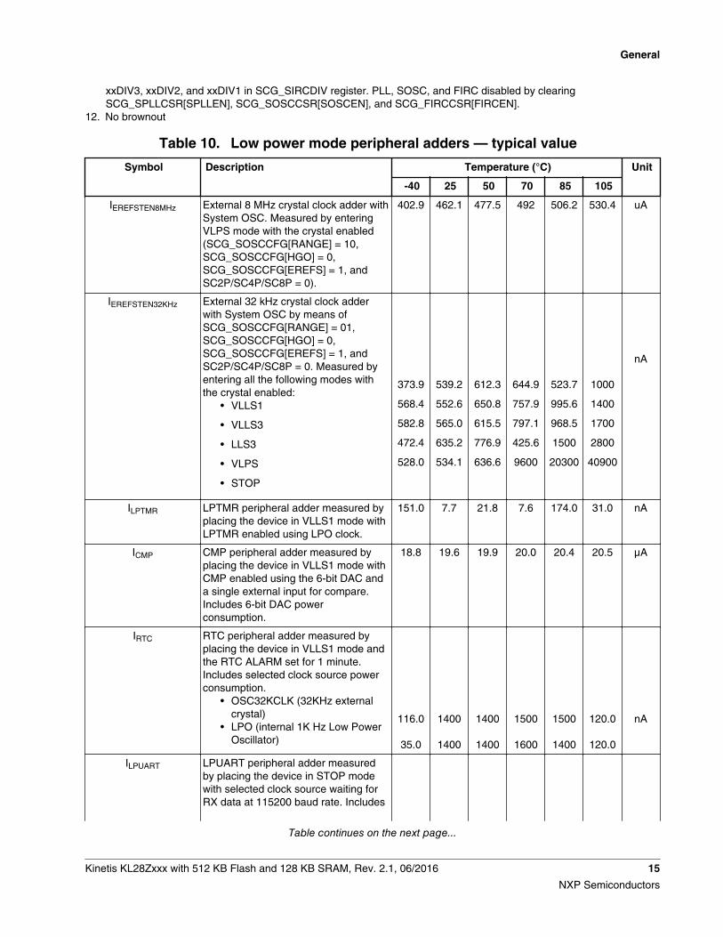
Table 10. Low power mode peripheral adders — typical value
Symbol Description Temperature (°C) Unit
-40 25 50 70 85 105
IEREFSTEN8MHz External 8 MHz crystal clock adder withSystem OSC. Measured by enteringVLPS mode with the crystal enabled(SCG_SOSCCFG[RANGE] = 10,SCG_SOSCCFG[HGO] = 0,SCG_SOSCCFG[EREFS] = 1, andSC2P/SC4P/SC8P = 0).
402.9 462.1 477.5 492 506.2 530.4 uA
IEREFSTEN32KHz External 32 kHz crystal clock adderwith System OSC by means ofSCG_SOSCCFG[RANGE] = 01,SCG_SOSCCFG[HGO] = 0,SCG_SOSCCFG[EREFS] = 1, andSC2P/SC4P/SC8P = 0. Measured byentering all the following modes withthe crystal enabled:
• VLLS1
• VLLS3
• LLS3
• VLPS
• STOP
373.9
568.4
582.8
472.4
528.0
539.2
552.6
565.0
635.2
534.1
612.3
650.8
615.5
776.9
636.6
644.9
757.9
797.1
425.6
9600
523.7
995.6
968.5
1500
20300
1000
1400
1700
2800
40900
nA
ILPTMR LPTMR peripheral adder measured byplacing the device in VLLS1 mode withLPTMR enabled using LPO clock.
151.0 7.7 21.8 7.6 174.0 31.0 nA
ICMP CMP peripheral adder measured byplacing the device in VLLS1 mode withCMP enabled using the 6-bit DAC anda single external input for compare.Includes 6-bit DAC powerconsumption.
18.8 19.6 19.9 20.0 20.4 20.5 µA
IRTC RTC peripheral adder measured byplacing the device in VLLS1 mode andthe RTC ALARM set for 1 minute.Includes selected clock source powerconsumption.
• OSC32KCLK (32KHz externalcrystal)
• LPO (internal 1K Hz Low PowerOscillator)
116.0
35.0
1400
1400
1400
1400
1500
1600
1500
1400
120.0
120.0
nA
ILPUART LPUART peripheral adder measuredby placing the device in STOP modewith selected clock source waiting forRX data at 115200 baud rate. Includes
Table continues on the next page...
General
Kinetis KL28Zxxx with 512 KB Flash and 128 KB SRAM, Rev. 2.1, 06/2016 15
NXP Semiconductors
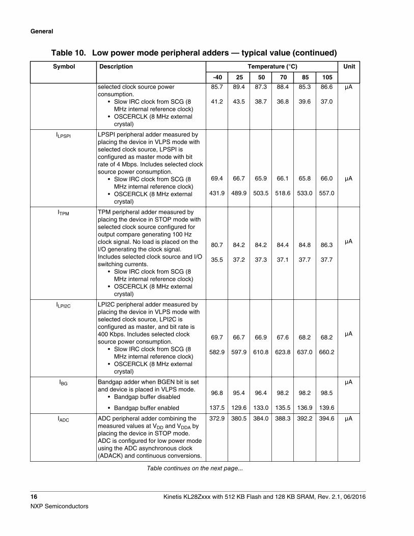
Table 10. Low power mode peripheral adders — typical value (continued)
Symbol Description Temperature (°C) Unit
-40 25 50 70 85 105
selected clock source powerconsumption.
• Slow IRC clock from SCG (8MHz internal reference clock)
• OSCERCLK (8 MHz externalcrystal)
85.7
41.2
89.4
43.5
87.3
38.7
88.4
36.8
85.3
39.6
86.6
37.0
µA
ILPSPI LPSPI peripheral adder measured byplacing the device in VLPS mode withselected clock source, LPSPI isconfigured as master mode with bitrate of 4 Mbps. Includes selected clocksource power consumption.
• Slow IRC clock from SCG (8MHz internal reference clock)
• OSCERCLK (8 MHz externalcrystal)
69.4
431.9
66.7
489.9
65.9
503.5
66.1
518.6
65.8
533.0
66.0
557.0
µA
ITPM TPM peripheral adder measured byplacing the device in STOP mode withselected clock source configured foroutput compare generating 100 Hzclock signal. No load is placed on theI/O generating the clock signal.Includes selected clock source and I/Oswitching currents.
• Slow IRC clock from SCG (8MHz internal reference clock)
• OSCERCLK (8 MHz externalcrystal)
80.7
35.5
84.2
37.2
84.2
37.3
84.4
37.1
84.8
37.7
86.3
37.7
µA
ILPI2C LPI2C peripheral adder measured byplacing the device in VLPS mode withselected clock source, LPI2C isconfigured as master, and bit rate is400 Kbps. Includes selected clocksource power consumption.
• Slow IRC clock from SCG (8MHz internal reference clock)
• OSCERCLK (8 MHz externalcrystal)
69.7
582.9
66.7
597.9
66.9
610.8
67.6
623.8
68.2
637.0
68.2
660.2
µA
IBG Bandgap adder when BGEN bit is setand device is placed in VLPS mode.
• Bandgap buffer disabled
• Bandgap buffer enabled
96.8
137.5
95.4
129.6
96.4
133.0
98.2
135.5
98.2
136.9
98.5
139.6
µA
IADC ADC peripheral adder combining themeasured values at VDD and VDDA byplacing the device in STOP mode.ADC is configured for low power modeusing the ADC asynchronous clock(ADACK) and continuous conversions.
372.9 380.5 384.0 388.3 392.2 394.6 µA
Table continues on the next page...
General
16 Kinetis KL28Zxxx with 512 KB Flash and 128 KB SRAM, Rev. 2.1, 06/2016
NXP Semiconductors
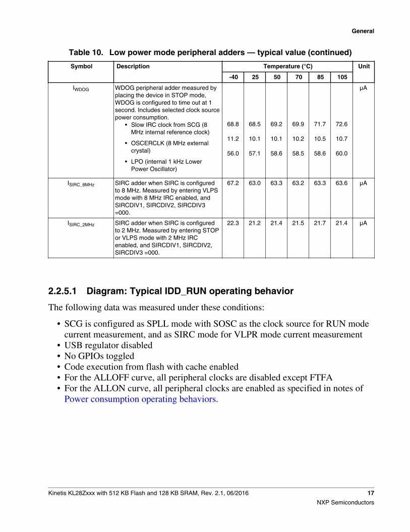
Table 10. Low power mode peripheral adders — typical value (continued)
Symbol Description Temperature (°C) Unit
-40 25 50 70 85 105
IWDOG WDOG peripheral adder measured byplacing the device in STOP mode,WDOG is configured to time out at 1second. Includes selected clock sourcepower consumption.
• Slow IRC clock from SCG (8MHz internal reference clock)
• OSCERCLK (8 MHz externalcrystal)
• LPO (internal 1 kHz LowerPower Oscillator)
68.8
11.2
56.0
68.5
10.1
57.1
69.2
10.1
58.6
69.9
10.2
58.5
71.7
10.5
58.6
72.6
10.7
60.0
µA
ISIRC_8MHz SIRC adder when SIRC is configuredto 8 MHz. Measured by entering VLPSmode with 8 MHz IRC enabled, andSIRCDIV1, SIRCDIV2, SIRCDIV3=000.
67.2 63.0 63.3 63.2 63.3 63.6 µA
ISIRC_2MHz SIRC adder when SIRC is configuredto 2 MHz. Measured by entering STOPor VLPS mode with 2 MHz IRCenabled, and SIRCDIV1, SIRCDIV2,SIRCDIV3 =000.
22.3 21.2 21.4 21.5 21.7 21.4 µA
2.2.5.1 Diagram: Typical IDD_RUN operating behavior
The following data was measured under these conditions:
• SCG is configured as SPLL mode with SOSC as the clock source for RUN modecurrent measurement, and as SIRC mode for VLPR mode current measurement
• USB regulator disabled• No GPIOs toggled• Code execution from flash with cache enabled• For the ALLOFF curve, all peripheral clocks are disabled except FTFA• For the ALLON curve, all peripheral clocks are enabled as specified in notes of
Power consumption operating behaviors.
General
Kinetis KL28Zxxx with 512 KB Flash and 128 KB SRAM, Rev. 2.1, 06/2016 17
NXP Semiconductors
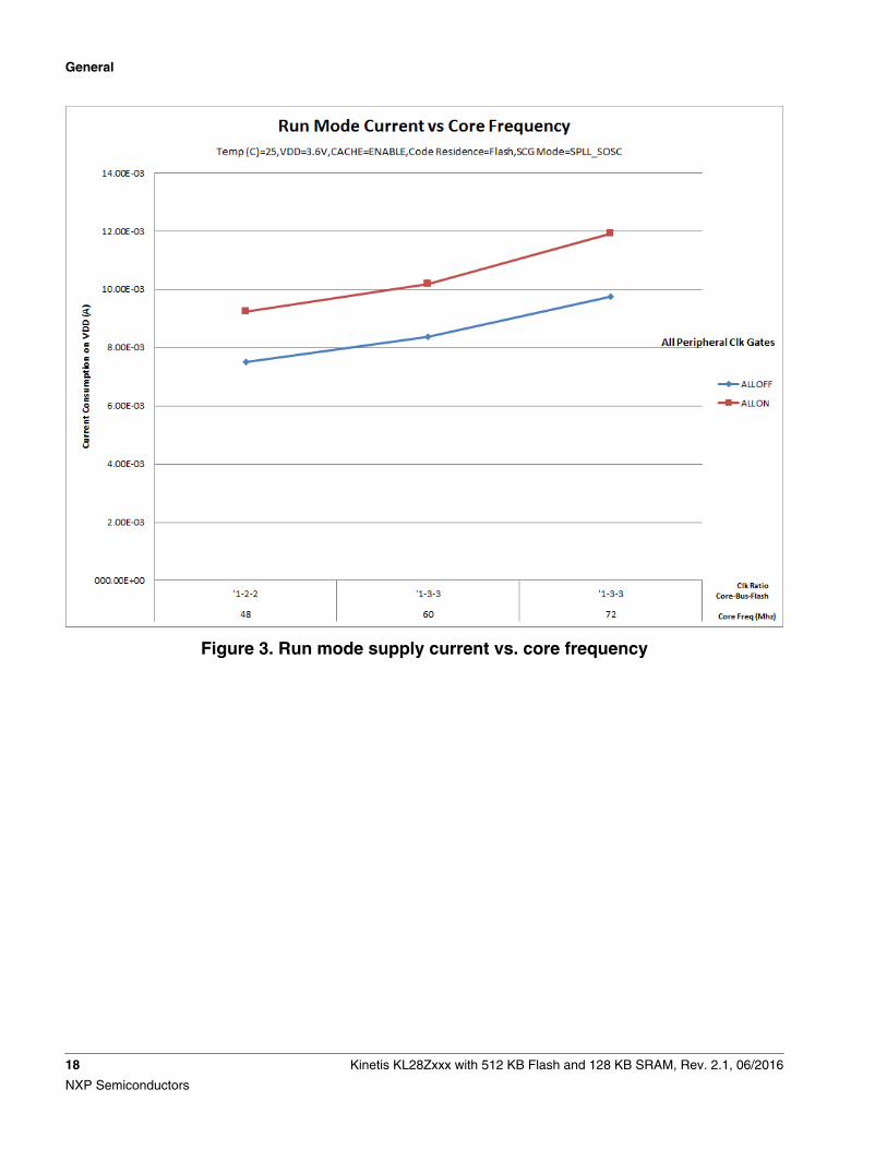
Figure 3. Run mode supply current vs. core frequency
General
18 Kinetis KL28Zxxx with 512 KB Flash and 128 KB SRAM, Rev. 2.1, 06/2016
NXP Semiconductors
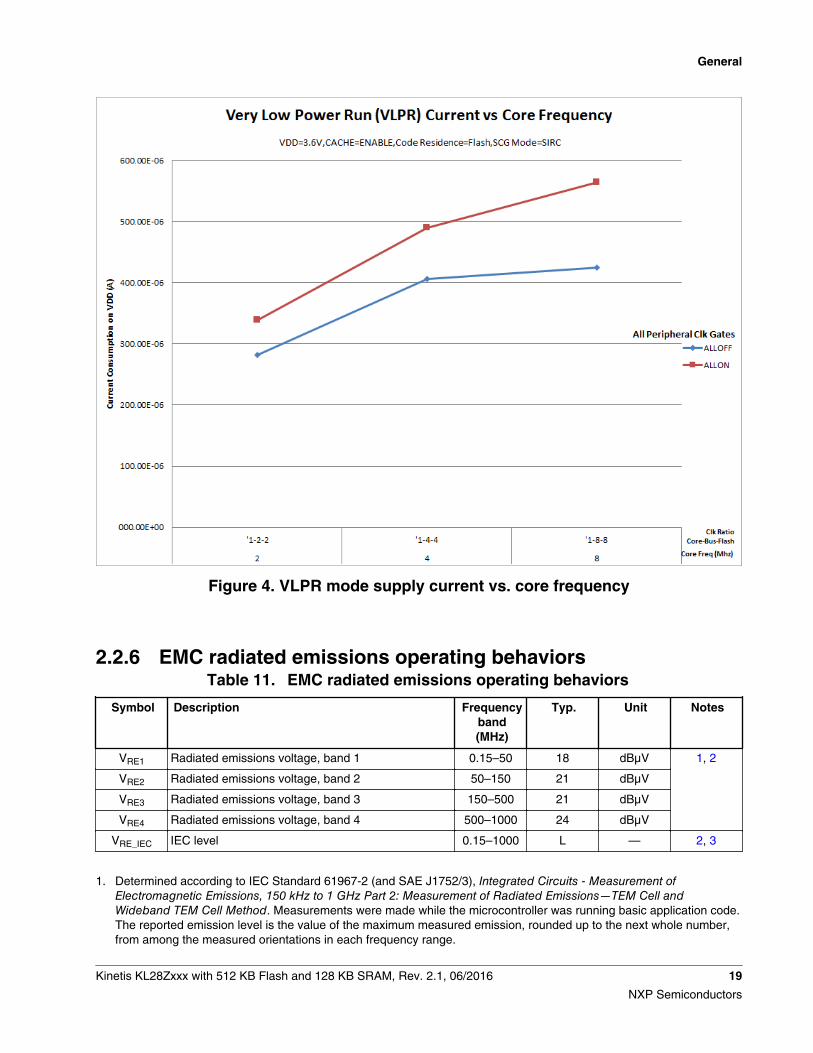
Figure 4. VLPR mode supply current vs. core frequency
2.2.6 EMC radiated emissions operating behaviorsTable 11. EMC radiated emissions operating behaviors
Symbol Description Frequencyband(MHz)
Typ. Unit Notes
VRE1 Radiated emissions voltage, band 1 0.15–50 18 dBμV 1, 2
VRE2 Radiated emissions voltage, band 2 50–150 21 dBμV
VRE3 Radiated emissions voltage, band 3 150–500 21 dBμV
VRE4 Radiated emissions voltage, band 4 500–1000 24 dBμV
VRE_IEC IEC level 0.15–1000 L — 2, 3
1. Determined according to IEC Standard 61967-2 (and SAE J1752/3), Integrated Circuits - Measurement ofElectromagnetic Emissions, 150 kHz to 1 GHz Part 2: Measurement of Radiated Emissions—TEM Cell andWideband TEM Cell Method. Measurements were made while the microcontroller was running basic application code.The reported emission level is the value of the maximum measured emission, rounded up to the next whole number,from among the measured orientations in each frequency range.
General
Kinetis KL28Zxxx with 512 KB Flash and 128 KB SRAM, Rev. 2.1, 06/2016 19
NXP Semiconductors
2. VDD = 3.3 V, VREGIN= 5V, TA = 25 °C, fOSC = 8 MHz (crystal), fSYS_CORE = 96 MHz, fBUS = 24 MHz3. IEC/SAE level maximum: L≤24dB mV
2.2.7 Designing with radiated emissions in mindTo find application notes that provide guidance on designing your system to minimizeinterference from radiated emissions:
1. Go to www.nxp.com.2. Perform a keyword search for “EMC design.”
2.2.8 Capacitance attributesTable 12. Capacitance attributes
Symbol Description Min. Max. Unit
CIN Input capacitance — 7 pF
2.3 Switching specifications
2.3.1 Device clock specificationsTable 13. Device clock specifications
Symbol Description Min. Max. Unit Run mode1
Normal run mode
fSYS System and core clock (DIVCORE_CLK) — 96 MHz High speed runmode
— 72 MHz Normal speed runmode
— 8 MHz VLPR mode
fBUS Bus clock/Slow clock (DIVSLOW_CLK) — 24 MHz High speed runmode and Normalspeed run mode
— 1 MHz VLPR mode
fFLASH Flash clock — 24 MHz High speed runmode and Normalspeed run mode
— 1 MHz VLPR mode
fLLWU LLWU clock — 1 KHz All modes
fRCM RCM clock — 1 KHz All modes
Table continues on the next page...
General
20 Kinetis KL28Zxxx with 512 KB Flash and 128 KB SRAM, Rev. 2.1, 06/2016
NXP Semiconductors
Table 13. Device clock specifications (continued)
Symbol Description Min. Max. Unit Run mode1
fWDOG, fTSI WDOG clock, TSI clock — 24 MHz High speed runmode and Normalspeed run mode
— 1 MHz VLPR mode
fADC ADC clock — 242 MHz High speed runmode and Normalspeed run mode
— 8 MHz VLPR mode
fRTC RTC clock — 32.768 KHz All modes
fTSTMR TSTMR clock — 1 MHz All modes
fLPTMR LPTMR clock — 24 MHz All modes
fTPM, fLPIT,fLPSPI, fLPI2C,
fLPUART,fEMVSIM, fSAI,
fFLEXIO
TPM clock, LPIT clock, LPSPI clock, LPI2C clock,LPUART clock, EMVSIM clock, SAI clock, FlexIOclock
— 96 MHz High speed runmode
— 72 MHz Normal speed runmode
— 8 MHz VLPR mode
fUSB USB clock — 48 MHz High speed runmode and Normalspeed run mode
— 0 MHz VLPR mode
fERCLK External reference clock — 48 MHz High speed runmode and Normalspeed run mode
16 MHz VLPR mode
fosc_hi_2 Oscillator crystal or resonator frequency — highfrequency mode (high range)(SCG_SOSCCFG[RANGE]=11)
— 32 MHz High speed runmode and Normalspeed run mode
— 16 MHz VLPR mode
fCAU, fGPIO CAU clock, GPIO clock — 96 MHz High speed runmode
— 72 MHz Normal speed runmode
— 8 MHz VLPR mode
1. Normal run mode, High speed run mode, and VLPR mode.2. See ADC electrical specifications
2.3.2 General switching specifications
These general-purpose specifications apply to all signals configured for GPIO, LPI2C,and LPUART signals.
General
Kinetis KL28Zxxx with 512 KB Flash and 128 KB SRAM, Rev. 2.1, 06/2016 21
NXP Semiconductors
Table 14. General switching specifications
Description Min. Max. Unit Notes
GPIO pin interrupt pulse width (digital glitch filter disabled) —Synchronous path
1.5 — Bus clockcycles
1
GPIO pin interrupt pulse width (digital glitch filter disabled,analog filter enabled) — Asynchronous path
100 — ns
GPIO pin interrupt pulse width (digital glitch filter disabled,analog filter disabled) — Asynchronous path
50 — ns
External RESET and NMI pin interrupt pulse width —Asynchronous path
100 — ns 2
GPIO pin interrupt pulse width — Asynchronous path 16 — ns 2
Port rise/fall time
Normal drive pins
• 2.7 ≤ VDD ≤ 3.6 V• Fast slew rate
• Slow slew rate• 1.71 ≤ VDD ≤ 2.7 V
• Fast slew rate
• Slow slew rate
—
—
—
—
3
10.5
4
17
ns
3
High drive pins
Normal/low drive enabled• 2.7 ≤ VDD ≤ 3.6 V
• Fast slew rate
• Slow slew rate• 1.71 ≤ VDD ≤ 2.7 V
• Fast slew rate
• Slow slew rate
High drive enabled• 2.7 ≤ VDD ≤ 3.6 V
• Fast slew rate
• Slow slew rate• 1.71 ≤ VDD ≤ 2.7 V
• Fast slew rate
• Slow slew rate
—
—
—
—
—
—
—
—
2.5
10.5
4
17
2
11
2.5
17
ns
4
Normal drive fast pins
• 2.7 ≤ VDD ≤ 3.6 V• Fast slew rate
• Slow slew rate• 1.71 ≤ VDD ≤ 2.7 V
• Fast slew rate
• Slow slew rate
—
—
—
—
0.5
10
0.75
19
ns
5
High drive fast pins
Normal/low drive enabled• 2.7 ≤ VDD ≤ 3.6 V
— 0.5 ns
6
General
22 Kinetis KL28Zxxx with 512 KB Flash and 128 KB SRAM, Rev. 2.1, 06/2016
NXP Semiconductors
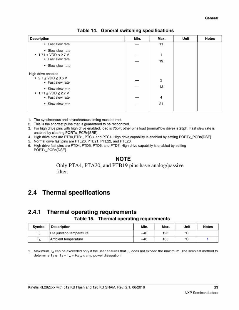
Table 14. General switching specifications
Description Min. Max. Unit Notes
• Fast slew rate
• Slow slew rate• 1.71 ≤ VDD ≤ 2.7 V
• Fast slew rate
• Slow slew rate
High drive enabled• 2.7 ≤ VDD ≤ 3.6 V
• Fast slew rate
• Slow slew rate• 1.71 ≤ VDD ≤ 2.7 V
• Fast slew rate
• Slow slew rate
—
—
—
—
—
—
—
11
1
19
2
13
4
21
1. The synchronous and asynchronous timing must be met.2. This is the shortest pulse that is guaranteed to be recognized.3. For high drive pins with high drive enabled, load is 75pF; other pins load (normal/low drive) is 25pF. Fast slew rate is
enabled by clearing PORTx_PCRn[SRE].4. High drive pins are PTB0,PTB1, PTC3, and PTC4. High drive capability is enabled by setting PORTx_PCRn[DSE].5. Normal drive fast pins are PTE20, PTE21, PTE22, and PTE23.6. High drive fast pins are PTD4, PTD5, PTD6, and PTD7. High drive capability is enabled by setting
PORTx_PCRn[DSE].
NOTEOnly PTA4, PTA20, and PTB19 pins have analog/passivefilter.
2.4 Thermal specifications
2.4.1 Thermal operating requirementsTable 15. Thermal operating requirements
Symbol Description Min. Max. Unit Notes
TJ Die junction temperature –40 125 °C
TA Ambient temperature –40 105 °C 1
1. Maximum TA can be exceeded only if the user ensures that TJ does not exceed the maximum. The simplest method todetermine TJ is: TJ = TA + RθJA × chip power dissipation.
General
Kinetis KL28Zxxx with 512 KB Flash and 128 KB SRAM, Rev. 2.1, 06/2016 23
NXP Semiconductors
2.4.2 Thermal attributesTable 16. Thermal attributes
Board type Symbol Description 100 LQFP 121XFBGA
Unit Notes
Single-layer (1S) RθJA Thermal resistance, junction toambient (natural convection)
64 94 °C/W 1
Four-layer (2s2p) RθJA Thermal resistance, junction toambient (natural convection)
51 57 °C/W
Single-layer (1S) RθJMA Thermal resistance, junction toambient (200 ft./min. air speed)
54 81 °C/W
Four-layer (2s2p) RθJMA Thermal resistance, junction toambient (200 ft./min. air speed)
45 53 °C/W
— RθJB Thermal resistance, junction toboard
37 40 °C/W 2
— RθJC Thermal resistance, junction tocase
19 30 °C/W 3
— ΨJT Thermal characterizationparameter, junction to package topoutside center (natural convection)
4 8 °C/W 4
1. Determined according to JEDEC Standard JESD51-2, Integrated Circuits Thermal Test Method EnvironmentalConditions—Natural Convection (Still Air), or EIA/JEDEC Standard JESD51-6, Integrated Circuit Thermal Test MethodEnvironmental Conditions—Forced Convection (Moving Air).
2. Determined according to JEDEC Standard JESD51-8, Integrated Circuit Thermal Test Method EnvironmentalConditions—Junction-to-Board.
3. Determined according to Method 1012.1 of MIL-STD 883, Test Method Standard, Microcircuits, with the cold platetemperature used for the case temperature. The value includes the thermal resistance of the interface material betweenthe top of the package and the cold plate.
4. Determined according to JEDEC Standard JESD51-2, Integrated Circuits Thermal Test Method EnvironmentalConditions—Natural Convection (Still Air).
3 Peripheral operating requirements and behaviors
3.1 Core modules
3.1.1 SWD electricalsTable 17. SWD full voltage range electricals
Symbol Description Min. Max. Unit
Operating voltage 1.71 3.6 V
J1 SWD_CLK frequency of operation
Table continues on the next page...
Peripheral operating requirements and behaviors
24 Kinetis KL28Zxxx with 512 KB Flash and 128 KB SRAM, Rev. 2.1, 06/2016
NXP Semiconductors
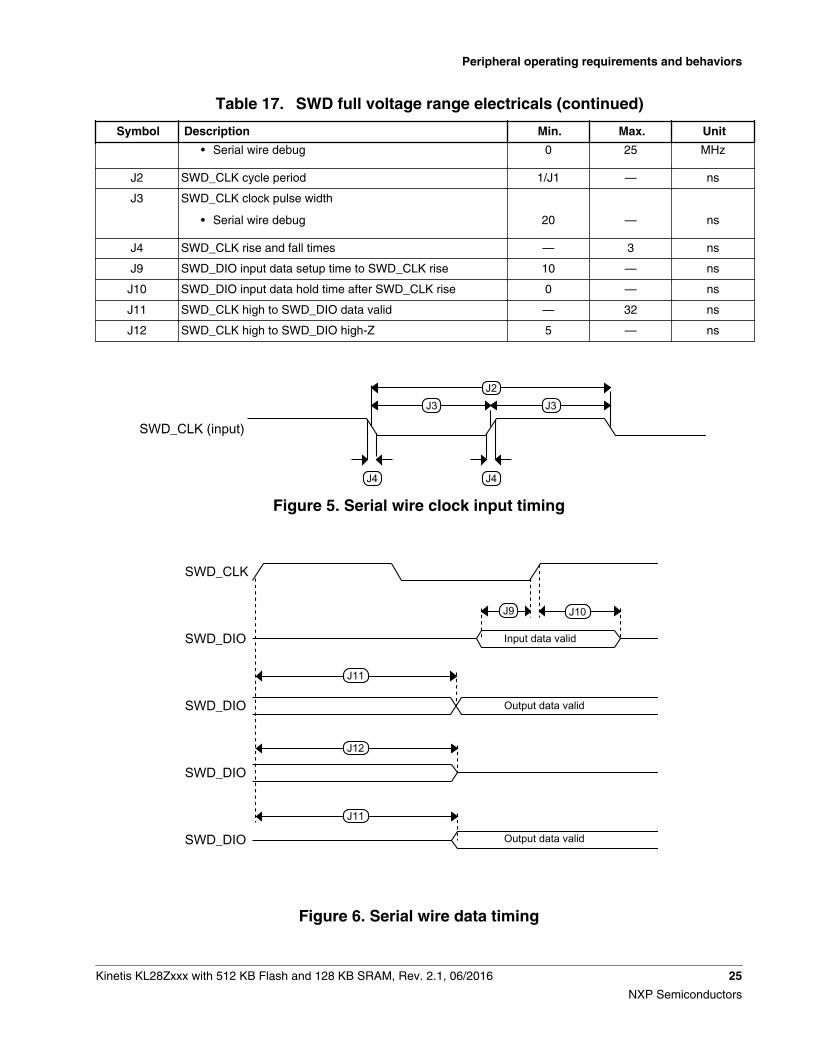
Table 17. SWD full voltage range electricals (continued)
Symbol Description Min. Max. Unit
• Serial wire debug 0 25 MHz
J2 SWD_CLK cycle period 1/J1 — ns
J3 SWD_CLK clock pulse width
• Serial wire debug
20
—
ns
J4 SWD_CLK rise and fall times — 3 ns
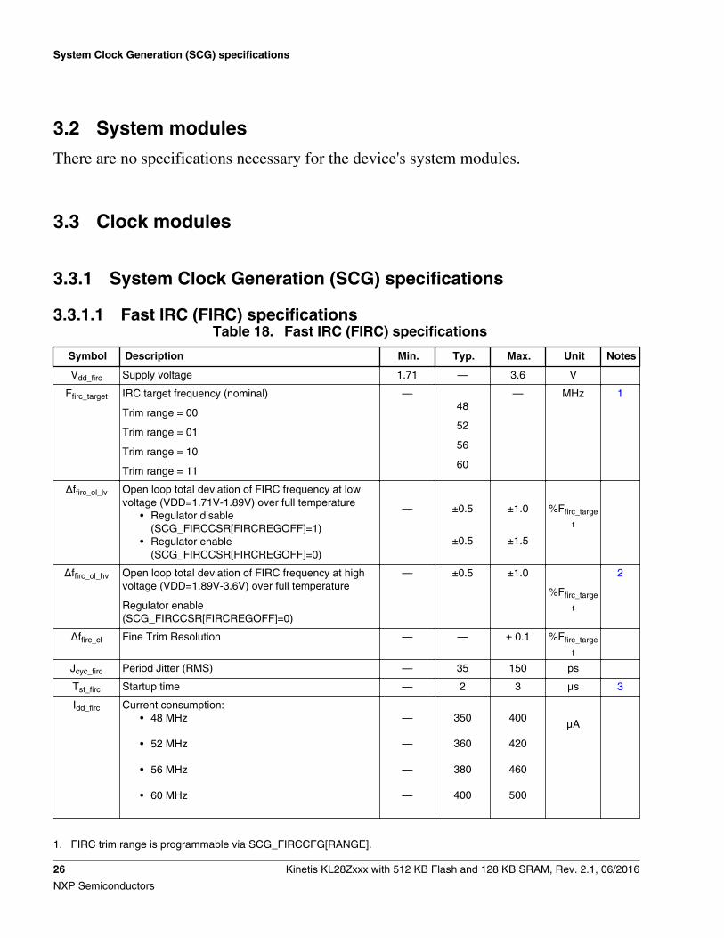
J9 SWD_DIO input data setup time to SWD_CLK rise 10 — ns
J10 SWD_DIO input data hold time after SWD_CLK rise 0 — ns
J11 SWD_CLK high to SWD_DIO data valid — 32 ns
J12 SWD_CLK high to SWD_DIO high-Z 5 — ns
J2J3 J3
J4 J4
SWD_CLK (input)
Figure 5. Serial wire clock input timing
J11
J12
J11
J9 J10
Input data valid
Output data valid
Output data valid
SWD_CLK
SWD_DIO
SWD_DIO
SWD_DIO
SWD_DIO
Figure 6. Serial wire data timing
Peripheral operating requirements and behaviors
Kinetis KL28Zxxx with 512 KB Flash and 128 KB SRAM, Rev. 2.1, 06/2016 25
NXP Semiconductors
3.2 System modules
There are no specifications necessary for the device's system modules.
3.3 Clock modules
System Clock Generation (SCG) specifications
3.3.1.1 Fast IRC (FIRC) specificationsTable 18. Fast IRC (FIRC) specifications
Symbol Description Min. Typ. Max. Unit Notes
Vdd_firc Supply voltage 1.71 — 3.6 V
Ffirc_target IRC target frequency (nominal)
Trim range = 00
Trim range = 01
Trim range = 10
Trim range = 11
—48
52
56
60
— MHz 1
Δffirc_ol_lv Open loop total deviation of FIRC frequency at lowvoltage (VDD=1.71V-1.89V) over full temperature
• Regulator disable(SCG_FIRCCSR[FIRCREGOFF]=1)
• Regulator enable(SCG_FIRCCSR[FIRCREGOFF]=0)
— ±0.5
±0.5
±1.0
±1.5
%Ffirc_targe
t
Δffirc_ol_hv Open loop total deviation of FIRC frequency at highvoltage (VDD=1.89V-3.6V) over full temperature
Regulator enable(SCG_FIRCCSR[FIRCREGOFF]=0)
— ±0.5 ±1.0
%Ffirc_targe
t
2
Δffirc_cl Fine Trim Resolution — — ± 0.1 %Ffirc_targe
t
Jcyc_firc Period Jitter (RMS) — 35 150 ps
Tst_firc Startup time — 2 3 μs 3
Idd_firc Current consumption:• 48 MHz
• 52 MHz
• 56 MHz
• 60 MHz
—
—
—
—
350
360
380
400
400
420
460
500
μA
1. FIRC trim range is programmable via SCG_FIRCCFG[RANGE].
3.3.1
System Clock Generation (SCG) specifications
26 Kinetis KL28Zxxx with 512 KB Flash and 128 KB SRAM, Rev. 2.1, 06/2016
NXP Semiconductors

2. Closed loop operation of the FIRC is only usable for USB device operation; it is not usable for USB host operation. It isenabled by configuring for USB Device, selecting FIRC as USB clock source, and enabling the clock recover function(USBn_CLK_RECOVER_CTRL[CLOCK_RECOVER_EN]=1, SCG_FIRCCSR[FIRCREGOFF]=0).
3. FIRC startup time is defined as the time between clock enablement and clock availability for system use.
3.3.1.2 Slow IRC (SIRC) specificationsTable 19. Slow IRC specifications
Symbol Description Min. Typ. Max. Unit Notes
IDD_sirc2M Supply current in 2 MHz mode — 14 17 μA
IDD_sirc8M Supply current in 8 MHz mode — 25 35 μA
fsirc Output frequency — 2 — MHz 1
— 8 —
Δfsirc Total deviation of trimmed frequency over voltageand temperature
• 0 to 105 °C
• -40 to 0 °C
—
—
—
—
±3
±4
%fsirc
2
Δfsirc_t Total deviation of trimmed frequency overtemperature @VDD=3.3V
—
—
±3
%fsirc
2
Tsu_sirc Startup time — — 12.5 μs
Jcyc_sirc Period jitter (RMS)• fsirc = 2 MHz• fsirc = 8 Mhz
—
—
350
100
—
—
ps 3
1. Selection of output frequency for Slow IRC between 2 MHz and 8 MHz is controlled by SCG_ SIRCCFG[RANGE].2. Maximum deviation occurs at cold temperature (-40 °C) and hot temperature (105 °C).3. This specification was obtained using a NXP developed PCB. Jitter is dependent on the noise characteristics of each
PCB and results will vary.
3.3.1.3 System PLL specificationsTable 20. System PLL Specifications
Symbol Description Min. Typ. Max. Unit Notes
fpll_ref PLL reference frequency range 8 — 16 MHz
fvcoclk_2x VCO output frequency 180 — 288 MHz
fvcoclk PLL output frequency 90 — 144 MHz
Ipll PLL operating current — VCO @ 180 MHz (f osc_hi_2= 10 MHz , f pll_ref = 10 MHz ,VDIV multiplier = 18)
—
1.1
—
mA
1
PLL operating current — VCO @ 288 MHz (f osc_hi_2= 32 MHz , f pll_ref = 8 MHz ,VDIV multiplier = 36)
—
2.0
—
Jcyc_pll PLL period jitter (RMS)• fvco = 180 MHz
• fvco = 288 MHz
—
—
120
80
—
—
ps2
Table continues on the next page...
System Clock Generation (SCG) specifications
Kinetis KL28Zxxx with 512 KB Flash and 128 KB SRAM, Rev. 2.1, 06/2016 27
NXP Semiconductors
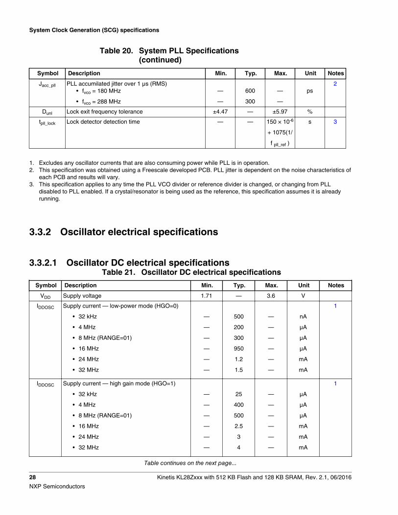
Table 20. System PLL Specifications(continued)
Symbol Description Min. Typ. Max. Unit Notes
Jacc_pll PLL accumilated jitter over 1 μs (RMS)• fvco = 180 MHz
• fvco = 288 MHz
—
—
600
300
—
—
ps2
Dunl Lock exit frequency tolerance ±4.47 — ±5.97 %
tpll_lock Lock detector detection time — — 150 × 10-6
+ 1075(1/
f pll_ref )
s 3
1. Excludes any oscillator currents that are also consuming power while PLL is in operation.2. This specification was obtained using a Freescale developed PCB. PLL jitter is dependent on the noise characteristics of
each PCB and results will vary.3. This specification applies to any time the PLL VCO divider or reference divider is changed, or changing from PLL
disabled to PLL enabled. If a crystal/resonator is being used as the reference, this specification assumes it is alreadyrunning.
3.3.2 Oscillator electrical specifications
3.3.2.1 Oscillator DC electrical specificationsTable 21. Oscillator DC electrical specifications
Symbol Description Min. Typ. Max. Unit Notes
VDD Supply voltage 1.71 — 3.6 V
IDDOSC Supply current — low-power mode (HGO=0)
• 32 kHz
• 4 MHz
• 8 MHz (RANGE=01)
• 16 MHz
• 24 MHz
• 32 MHz
—
—
—
—
—
—
500
200
300
950
1.2
1.5
—
—
—
—
—
—
nA
μA
μA
μA
mA
mA
1
IDDOSC Supply current — high gain mode (HGO=1)
• 32 kHz
• 4 MHz
• 8 MHz (RANGE=01)
• 16 MHz
• 24 MHz
• 32 MHz
—
—
—
—
—
—
25
400
500
2.5
3
4
—
—
—
—
—
—
μA
μA
μA
mA
mA
mA
1
Table continues on the next page...
System Clock Generation (SCG) specifications
28 Kinetis KL28Zxxx with 512 KB Flash and 128 KB SRAM, Rev. 2.1, 06/2016
NXP Semiconductors
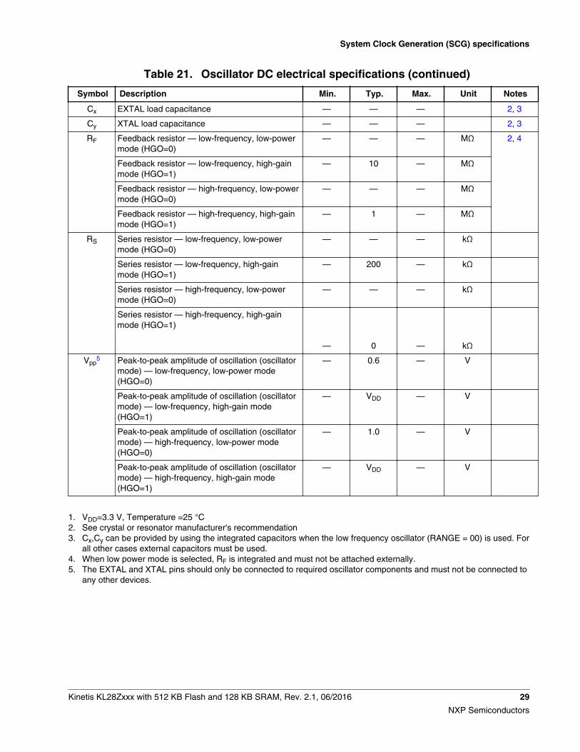
Table 21. Oscillator DC electrical specifications (continued)
Symbol Description Min. Typ. Max. Unit Notes
Cx EXTAL load capacitance — — — 2, 3
Cy XTAL load capacitance — — — 2, 3
RF Feedback resistor — low-frequency, low-powermode (HGO=0)
— — — MΩ 2, 4
Feedback resistor — low-frequency, high-gainmode (HGO=1)
— 10 — MΩ
Feedback resistor — high-frequency, low-powermode (HGO=0)
— — — MΩ
Feedback resistor — high-frequency, high-gainmode (HGO=1)
— 1 — MΩ
RS Series resistor — low-frequency, low-powermode (HGO=0)
— — — kΩ
Series resistor — low-frequency, high-gainmode (HGO=1)
— 200 — kΩ
Series resistor — high-frequency, low-powermode (HGO=0)
— — — kΩ
Series resistor — high-frequency, high-gainmode (HGO=1)
—
0
—
kΩ
Vpp5 Peak-to-peak amplitude of oscillation (oscillator
mode) — low-frequency, low-power mode(HGO=0)
— 0.6 — V
Peak-to-peak amplitude of oscillation (oscillatormode) — low-frequency, high-gain mode(HGO=1)
— VDD — V
Peak-to-peak amplitude of oscillation (oscillatormode) — high-frequency, low-power mode(HGO=0)
— 1.0 — V
Peak-to-peak amplitude of oscillation (oscillatormode) — high-frequency, high-gain mode(HGO=1)
— VDD — V
1. VDD=3.3 V, Temperature =25 °C2. See crystal or resonator manufacturer's recommendation3. Cx,Cy can be provided by using the integrated capacitors when the low frequency oscillator (RANGE = 00) is used. For
all other cases external capacitors must be used.4. When low power mode is selected, RF is integrated and must not be attached externally.5. The EXTAL and XTAL pins should only be connected to required oscillator components and must not be connected to
any other devices.
System Clock Generation (SCG) specifications
Kinetis KL28Zxxx with 512 KB Flash and 128 KB SRAM, Rev. 2.1, 06/2016 29
NXP Semiconductors
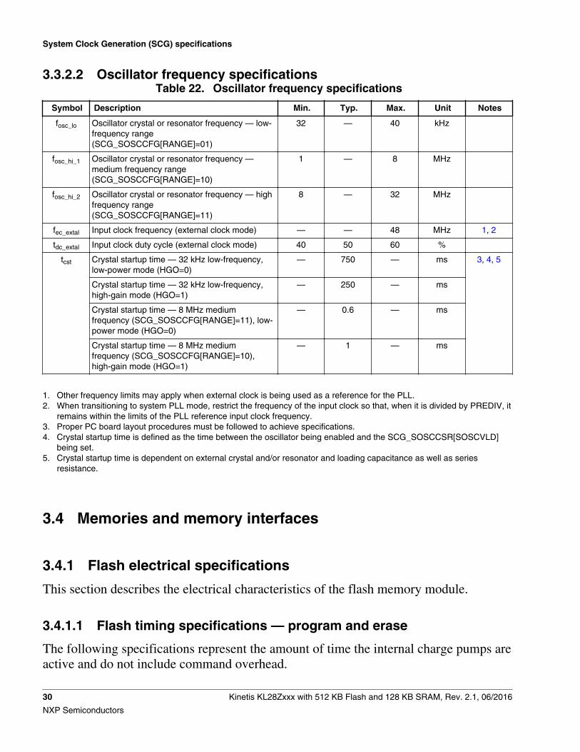
3.3.2.2 Oscillator frequency specificationsTable 22. Oscillator frequency specifications
Symbol Description Min. Typ. Max. Unit Notes
fosc_lo Oscillator crystal or resonator frequency — low-frequency range(SCG_SOSCCFG[RANGE]=01)
32 — 40 kHz
fosc_hi_1 Oscillator crystal or resonator frequency —medium frequency range(SCG_SOSCCFG[RANGE]=10)
1 — 8 MHz
fosc_hi_2 Oscillator crystal or resonator frequency — highfrequency range(SCG_SOSCCFG[RANGE]=11)
8 — 32 MHz
fec_extal Input clock frequency (external clock mode) — — 48 MHz 1, 2
tdc_extal Input clock duty cycle (external clock mode) 40 50 60 %
tcst Crystal startup time — 32 kHz low-frequency,low-power mode (HGO=0)
— 750 — ms 3, 4, 5
Crystal startup time — 32 kHz low-frequency,high-gain mode (HGO=1)
— 250 — ms
Crystal startup time — 8 MHz mediumfrequency (SCG_SOSCCFG[RANGE]=11), low-power mode (HGO=0)
— 0.6 — ms
Crystal startup time — 8 MHz mediumfrequency (SCG_SOSCCFG[RANGE]=10),high-gain mode (HGO=1)
— 1 — ms
1. Other frequency limits may apply when external clock is being used as a reference for the PLL.2. When transitioning to system PLL mode, restrict the frequency of the input clock so that, when it is divided by PREDIV, it
remains within the limits of the PLL reference input clock frequency.3. Proper PC board layout procedures must be followed to achieve specifications.4. Crystal startup time is defined as the time between the oscillator being enabled and the SCG_SOSCCSR[SOSCVLD]
being set.5. Crystal startup time is dependent on external crystal and/or resonator and loading capacitance as well as series
resistance.
3.4 Memories and memory interfaces
3.4.1 Flash electrical specifications
This section describes the electrical characteristics of the flash memory module.
3.4.1.1 Flash timing specifications — program and erase
The following specifications represent the amount of time the internal charge pumps areactive and do not include command overhead.
System Clock Generation (SCG) specifications
30 Kinetis KL28Zxxx with 512 KB Flash and 128 KB SRAM, Rev. 2.1, 06/2016
NXP Semiconductors
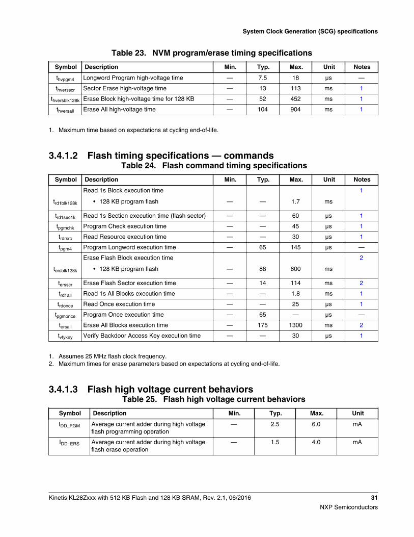
Table 23. NVM program/erase timing specifications
Symbol Description Min. Typ. Max. Unit Notes
thvpgm4 Longword Program high-voltage time — 7.5 18 μs —
thversscr Sector Erase high-voltage time — 13 113 ms 1
thversblk128k Erase Block high-voltage time for 128 KB — 52 452 ms 1
thversall Erase All high-voltage time — 104 904 ms 1
1. Maximum time based on expectations at cycling end-of-life.
3.4.1.2 Flash timing specifications — commandsTable 24. Flash command timing specifications
Symbol Description Min. Typ. Max. Unit Notes
trd1blk128k
Read 1s Block execution time
• 128 KB program flash
—
—
1.7
ms
1
trd1sec1k Read 1s Section execution time (flash sector) — — 60 μs 1
tpgmchk Program Check execution time — — 45 μs 1
trdrsrc Read Resource execution time — — 30 μs 1
tpgm4 Program Longword execution time — 65 145 μs —
tersblk128k
Erase Flash Block execution time
• 128 KB program flash
—
88
600
ms
2
tersscr Erase Flash Sector execution time — 14 114 ms 2
trd1all Read 1s All Blocks execution time — — 1.8 ms 1
trdonce Read Once execution time — — 25 μs 1
tpgmonce Program Once execution time — 65 — μs —
tersall Erase All Blocks execution time — 175 1300 ms 2
tvfykey Verify Backdoor Access Key execution time — — 30 μs 1
1. Assumes 25 MHz flash clock frequency.2. Maximum times for erase parameters based on expectations at cycling end-of-life.
3.4.1.3 Flash high voltage current behaviorsTable 25. Flash high voltage current behaviors
Symbol Description Min. Typ. Max. Unit
IDD_PGM Average current adder during high voltageflash programming operation
— 2.5 6.0 mA
IDD_ERS Average current adder during high voltageflash erase operation
— 1.5 4.0 mA
System Clock Generation (SCG) specifications
Kinetis KL28Zxxx with 512 KB Flash and 128 KB SRAM, Rev. 2.1, 06/2016 31
NXP Semiconductors
3.4.1.4 Reliability specificationsTable 26. NVM reliability specifications
Symbol Description Min. Typ.1 Max. Unit Notes
Program Flash
tnvmretp10k Data retention after up to 10 K cycles 5 50 — years —
tnvmretp1k Data retention after up to 1 K cycles 20 100 — years —
nnvmcycp Cycling endurance 10 K 50 K — cycles 2
1. Typical data retention values are based on measured response accelerated at high temperature and derated to aconstant 25 °C use profile. Engineering Bulletin EB618 does not apply to this technology. Typical endurance defined inEngineering Bulletin EB619.
2. Cycling endurance represents number of program/erase cycles at –40 °C ≤ Tj ≤ 125 °C.
3.5 Security and integrity modules
There are no specifications necessary for the device's security and integrity modules.
3.6 Analog
ADC electrical specifications
3.6.1.1 16-bit ADC operating conditionsTable 27. 16-bit ADC operating conditions
Symbol Description Conditions Min. Typ.1 Max. Unit Notes
VDDA Supply voltage Absolute 1.71 — 3.6 V —
ΔVDDA Supply voltage Delta to VDD (VDD – VDDA) -100 0 +100 mV 2
ΔVSSA Ground voltage Delta to VSS (VSS – VSSA) -100 0 +100 mV 2
VADIN Input voltage • 16-bit differential mode
• All other modes
VREFL
VREFL
—
—
31/32 ×VREFH
VREFH
V —
CADIN Inputcapacitance
• 16-bit mode
• 8-bit / 10-bit / 12-bitmodes
—
—
8
4
10
5
pF —
RADIN Input seriesresistance
— 2 5 kΩ —
RAS Analog sourceresistance
16-bit modes
• fADCK > 8 MHz
—
—
0.5
kΩ
3, 4
Table continues on the next page...
3.6.1
ADC electrical specifications
32 Kinetis KL28Zxxx with 512 KB Flash and 128 KB SRAM, Rev. 2.1, 06/2016
NXP Semiconductors
Table 27. 16-bit ADC operating conditions (continued)
Symbol Description Conditions Min. Typ.1 Max. Unit Notes
• fADCK = 4–8 MHz
• fADCK < 4 MHz
13-bit / 12-bit modes
• fADCK > 16 MHz
• fADCK > 8 MHz
• fADCK = 4–8 MHz
• fADCK < 4 MHz
11-bit / 10-bit modes
• fADCK > 8 MHz
• fADCK = 4–8 MHz
• fADCK < 4MHz
9-bit / 8-bit modes• fADCK > 8 MHz• fADCK < 8 MHz
—
—
—
—
—
—
—
—
—
—
—
—
—
—
—
—
—
—
—
—
—
—
1
2
0.5
1
2
5
2
5
10
5
10
kΩ
kΩ
kΩ
kΩ
kΩ
kΩ
kΩ
kΩ
kΩ
kΩ
kΩ
fADCK ADC conversionclock frequency
≤ 13-bit mode 1.0 — 24.0 MHz 5
16-bit mode 2.0 — 12.0 MHz
Crate ADC conversionrate
≤ 13-bit modes
No ADC hardware averaging
Continuous conversionsenabled, subsequentconversion time
20.000
—
1200
ksps
6
Crate ADC conversionrate
16-bit mode
No ADC hardware averaging
Continuous conversionsenabled, subsequentconversion time
37.037
—
461.467
ksps
6
1. Typical values assume VDDA = 3.0 V, Temp = 25 °C, fADCK = 1.0 MHz, unless otherwise stated. Typical values are forreference only, and are not tested in production.
2. DC potential difference.3. Assumes ADLSMP=04. This resistance is external to the MCU. To achieve the best results, the analog source resistance must be kept as low
as possible. The results in this data sheet were derived from a system that had < 8 Ω analog source resistance. TheRAS * CAS time constant should be kept to < 1 ns.
5. To use the maximum ADC conversion clock frequency, CFG2[ADHSC] must be set and CFG1[ADLPC] must be clear.6. For guidelines and examples of conversion rate calculation, download the ADC calculator tool.
ADC electrical specifications
Kinetis KL28Zxxx with 512 KB Flash and 128 KB SRAM, Rev. 2.1, 06/2016 33
NXP Semiconductors
RAS
VAS CAS
ZAS
VADIN
ZADIN
RADIN
RADIN
RADIN
RADIN
CADIN
Pad leakagedue toinput protection
INPUT PIN
INPUT PIN
INPUT PIN
SIMPLIFIEDINPUT PIN EQUIVALENT
CIRCUITSIMPLIFIED
CHANNEL SELECTCIRCUIT ADC SAR
ENGINE
Figure 7. ADC input impedance equivalency diagram
3.6.1.2 16-bit ADC electrical characteristics
Table 28. 16-bit ADC characteristics (VREFH = VDDA, VREFL = VSSA)
Symbol Description Conditions1 Min. Typ.2 Max. Unit Notes
IDDA_ADC Supply current 0.215 — 1.7 mA 3
fADACK
ADC asynchronousclock source
• ADLPC = 1, ADHSC = 0
• ADLPC = 1, ADHSC = 1
• ADLPC = 0, ADHSC = 0
• ADLPC = 0, ADHSC = 1
1.2
2.4
3.0
4.4
2.4
4.0
5.2
6.2
3.9
6.1
7.3
9.5
MHz
MHz
MHz
MHz
tADACK = 1/fADACK
Sample Time See Reference Manual chapter for sample times
TUE Total unadjustederror
• 12-bit modes
• <12-bit modes
—
—
±4
±1.4
±6.8
±2.1
LSB4 5
DNL Differential non-linearity
• 12-bit modes
• <12-bit modes
—
—
±0.7
±0.2
–1.1 to+1.9
–0.3 to0.5
LSB4 5
INL Integral non-linearity • 12-bit modes
• <12-bit modes
—
—
±1.0
±0.5
–2.7 to+1.9
LSB4 5
Table continues on the next page...
ADC electrical specifications
34 Kinetis KL28Zxxx with 512 KB Flash and 128 KB SRAM, Rev. 2.1, 06/2016
NXP Semiconductors
Table 28. 16-bit ADC characteristics (VREFH = VDDA, VREFL = VSSA) (continued)
Symbol Description Conditions1 Min. Typ.2 Max. Unit Notes
–0.7 to+0.5
EFS Full-scale error • 12-bit modes
• <12-bit modes
—
—
–4
–1.4
–5.4
–1.8
LSB4 VADIN = VDDA5
EQ Quantization error • 16-bit modes
• ≤13-bit modes
—
—
–1 to 0
—
—
±0.5
LSB4
ENOB Effective number ofbits
16-bit differential mode
• Avg = 32
• Avg = 4
16-bit single-ended mode
• Avg = 32
• Avg = 4
12.8
11.9
12.2
11.4
14.5
13.8
13.9
13.1
—
—
—
—
bits
bits
bits
bits
6
SINADSignal-to-noise plusdistortion
See ENOB6.02 × ENOB + 1.76 dB
THD Total harmonicdistortion
16-bit differential mode
• Avg = 32
16-bit single-ended mode
• Avg = 32
—
—
-94
-85
—
—
dB
dB
7
SFDR Spurious freedynamic range
16-bit differential mode
• Avg = 32
16-bit single-ended mode
• Avg = 32
82
78
95
90
—
—
dB
dB
7
EIL Input leakage error IIn × RAS mV IIn = leakagecurrent
(refer to theMCU's voltage
and currentoperatingratings)
Temp sensor slope Across the full temperaturerange of the device
1.55 1.62 1.69 mV/°C 8
VTEMP25 Temp sensor voltage 25 °C 706 716 726 mV 8
1. All accuracy numbers assume the ADC is calibrated with VREFH = VDDA2. Typical values assume VDDA = 3.0 V, Temp = 25 °C, fADCK = 2.0 MHz unless otherwise stated. Typical values are for
reference only and are not tested in production.3. The ADC supply current depends on the ADC conversion clock speed, conversion rate and ADC_CFG1[ADLPC] (low
power). For lowest power operation, ADC_CFG1[ADLPC] must be set, the ADC_CFG2[ADHSC] bit must be clear with1 MHz ADC conversion clock speed.
ADC electrical specifications
Kinetis KL28Zxxx with 512 KB Flash and 128 KB SRAM, Rev. 2.1, 06/2016 35
NXP Semiconductors
4. 1 LSB = (VREFH - VREFL)/2N
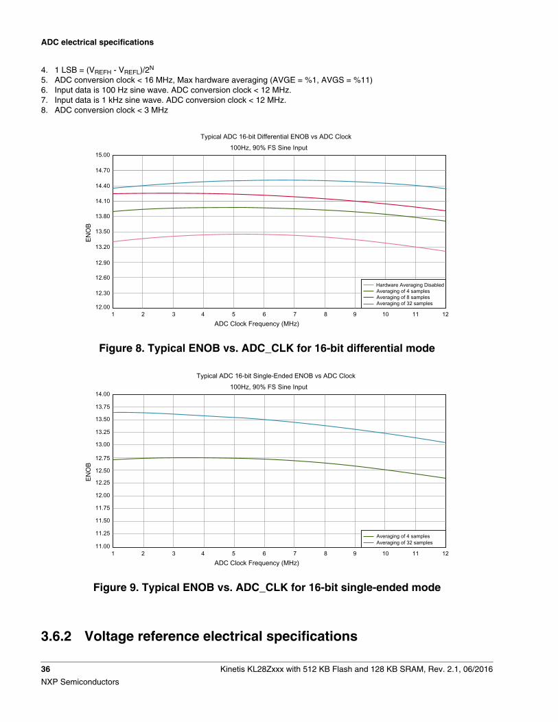
5. ADC conversion clock < 16 MHz, Max hardware averaging (AVGE = %1, AVGS = %11)6. Input data is 100 Hz sine wave. ADC conversion clock < 12 MHz.7. Input data is 1 kHz sine wave. ADC conversion clock < 12 MHz.8. ADC conversion clock < 3 MHz
Typical ADC 16-bit Differential ENOB vs ADC Clock100Hz, 90% FS Sine Input
ENO
B
ADC Clock Frequency (MHz)
15.00
14.70
14.40
14.10
13.80
13.50
13.20
12.90
12.60
12.30
12.001 2 3 4 5 6 7 8 9 10 1211
Hardware Averaging DisabledAveraging of 4 samplesAveraging of 8 samplesAveraging of 32 samples
Figure 8. Typical ENOB vs. ADC_CLK for 16-bit differential mode
Typical ADC 16-bit Single-Ended ENOB vs ADC Clock100Hz, 90% FS Sine Input
ENO
B
ADC Clock Frequency (MHz)
14.00
13.75
13.25
13.00
12.75
12.50
12.00
11.75
11.50
11.25
11.001 2 3 4 5 6 7 8 9 10 1211
Averaging of 4 samplesAveraging of 32 samples
13.50
12.25
Figure 9. Typical ENOB vs. ADC_CLK for 16-bit single-ended mode
3.6.2 Voltage reference electrical specifications
ADC electrical specifications
36 Kinetis KL28Zxxx with 512 KB Flash and 128 KB SRAM, Rev. 2.1, 06/2016
NXP Semiconductors

Table 29. VREF full-range operating requirements
Symbol Description Min. Max. Unit Notes
VDDA Supply voltage for 1.2V output 3.6 V —
Supply voltage for 2.1V output 2.4 3.6 V —
TA Temperature Operating temperaturerange of the device
°C —
CL Output load capacitance 100 nF 1, 2
1. CL must be connected to VREF_OUT if the VREF_OUT functionality is being used for either an internal or externalreference.
2. The load capacitance should not exceed +/-25% of the nominal specified CL value over the operating temperaturerange of the device.
Table 30. VREF full-range operating behaviors
Symbol Description Min. Typ. Max. Unit Notes
Vout Voltage reference output with factory trim atnominal VDDA and temperature=25°C
1.190 1.195 1.2 V 1
2.092 2.1 2.108 V
Vout Voltage reference 1.2 V output— factory trim 1.188 1.195 1.202 V 1
Voltage reference 2.1 V output — factory trim 2.087 2.1 2.113 V 1
Vstep Voltage reference trim step for 1.2 V output — 0.5 — mV 1
Voltage reference trim step for 2.1 V output — 1.5 — mV 1
Ac Aging coefficient — — 400 uV/yr —
Ibg Bandgap only current — 60 80 µA 1
Ilp Low-power buffer current — 180 360 µA 1
Ihp High-power buffer current — 480 960 µA 1
ΔVLOAD Load regulation — current is ± 1.0 mA — ±0.2 — mV 1, 2
Tstup Buffer startup time — — 100 µs —
Vvdrift Voltage drift for 1.2 V output (Vmax -Vminacross the full voltage range)
— 0.5 2 mV 1
Voltage drift for 2.1 V output (Vmax -Vminacross the full voltage range)
— 0.9 3.5 mV
Vtdrift Temperature drift for 1.2 V output (Vmax -Vminacross the full temperature range)
— 2 15 mV 3
Temperature drift for 2.1 V output (Vmax -Vminacross the full temperature range)
— 3.5 26 mV
1. See the chip's Reference Manual for the appropriate settings of the VREF Status and Control register for Voutselection of 1.2 V or 2.1 V.
2. Load regulation voltage is the difference between the VREF_OUT voltage with no load vs. voltage with defined load3. To get best performance of VREF temperature drift, VREF_SC[ICOMPEN] must be set.
Table 31. VREF limited-range operating requirements
Symbol Description Min. Max. Unit Notes
TA Temperature 0 50 °C —
ADC electrical specifications
Kinetis KL28Zxxx with 512 KB Flash and 128 KB SRAM, Rev. 2.1, 06/2016 37
NXP Semiconductors
Table 32. VREF limited-range operating behaviors
Symbol Description Min. Max. Unit Notes
Vout Voltage reference output 1.2 V with factory trim 1.173 1.225 V —
Vout Voltage reference output 2.1 V with factory trim 2.088 2.115 V —
3.6.3 CMP and 6-bit DAC electrical specificationsTable 33. Comparator and 6-bit DAC electrical specifications
Symbol Description Min. Typ. Max. Unit
VDD Supply voltage 1.71 — 3.6 V
IDDHS Supply current, High-speed mode (EN=1, PMODE=1) — — 200 μA
IDDLS Supply current, low-speed mode (EN=1, PMODE=0) — — 20 μA
VAIN Analog input voltage VSS – 0.3 — VDD V
VAIO Analog input offset voltage — — 20 mV
VH Analog comparator hysteresis1
• CR0[HYSTCTR] = 00
• CR0[HYSTCTR] = 01
• CR0[HYSTCTR] = 10
• CR0[HYSTCTR] = 11
—
—
—
—
5
10
20
30
—
—
—
—
mV
mV
mV
mV
VCMPOh Output high VDD – 0.5 — — V
VCMPOl Output low — — 0.5 V
tDHS Propagation delay, high-speed mode (EN=1, PMODE=1) 20 50 200 ns
tDLS Propagation delay, low-speed mode (EN=1, PMODE=0) 80 250 600 ns
Analog comparator initialization delay2 — — 40 μs
IDAC6b 6-bit DAC current adder (enabled) — 7 — μA
INL 6-bit DAC integral non-linearity –0.5 — 0.5 LSB3
DNL 6-bit DAC differential non-linearity –0.3 — 0.3 LSB
1. Typical hysteresis is measured with input voltage range limited to 0.6 to VDD–0.6 V.2. Comparator initialization delay is defined as the time between software writes to change control inputs (Writes to
CMP_DACCR[DACEN], CMP_DACCR[VRSEL], CMP_DACCR[VOSEL], CMP_MUXCR[PSEL], andCMP_MUXCR[MSEL]) and the comparator output settling to a stable level.
3. 1 LSB = Vreference/64
ADC electrical specifications
38 Kinetis KL28Zxxx with 512 KB Flash and 128 KB SRAM, Rev. 2.1, 06/2016
NXP Semiconductors
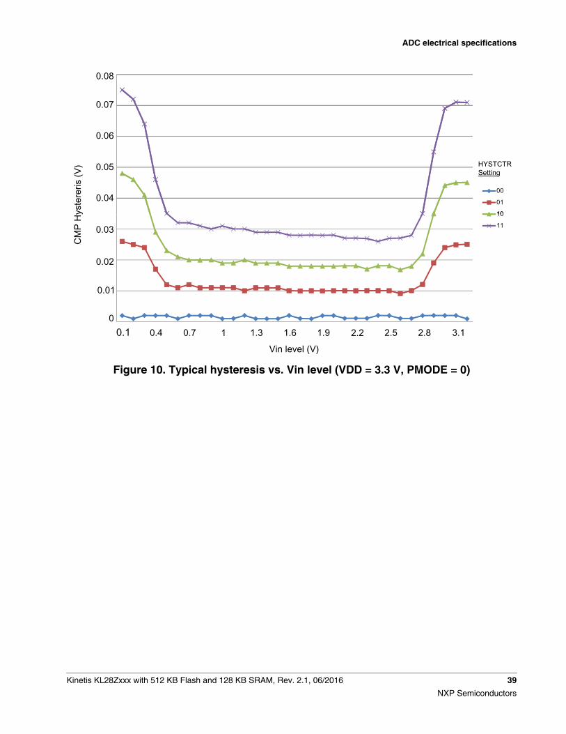
00
01
10
HYSTCTR Setting
0.1
10
11
Vin level (V)
CM
P H
yste
reris
(V)
3.12.82.52.21.91.61.310.70.4
0.05
0
0.01
0.02
0.03
0.08
0.07
0.06
0.04
Figure 10. Typical hysteresis vs. Vin level (VDD = 3.3 V, PMODE = 0)
ADC electrical specifications
Kinetis KL28Zxxx with 512 KB Flash and 128 KB SRAM, Rev. 2.1, 06/2016 39
NXP Semiconductors
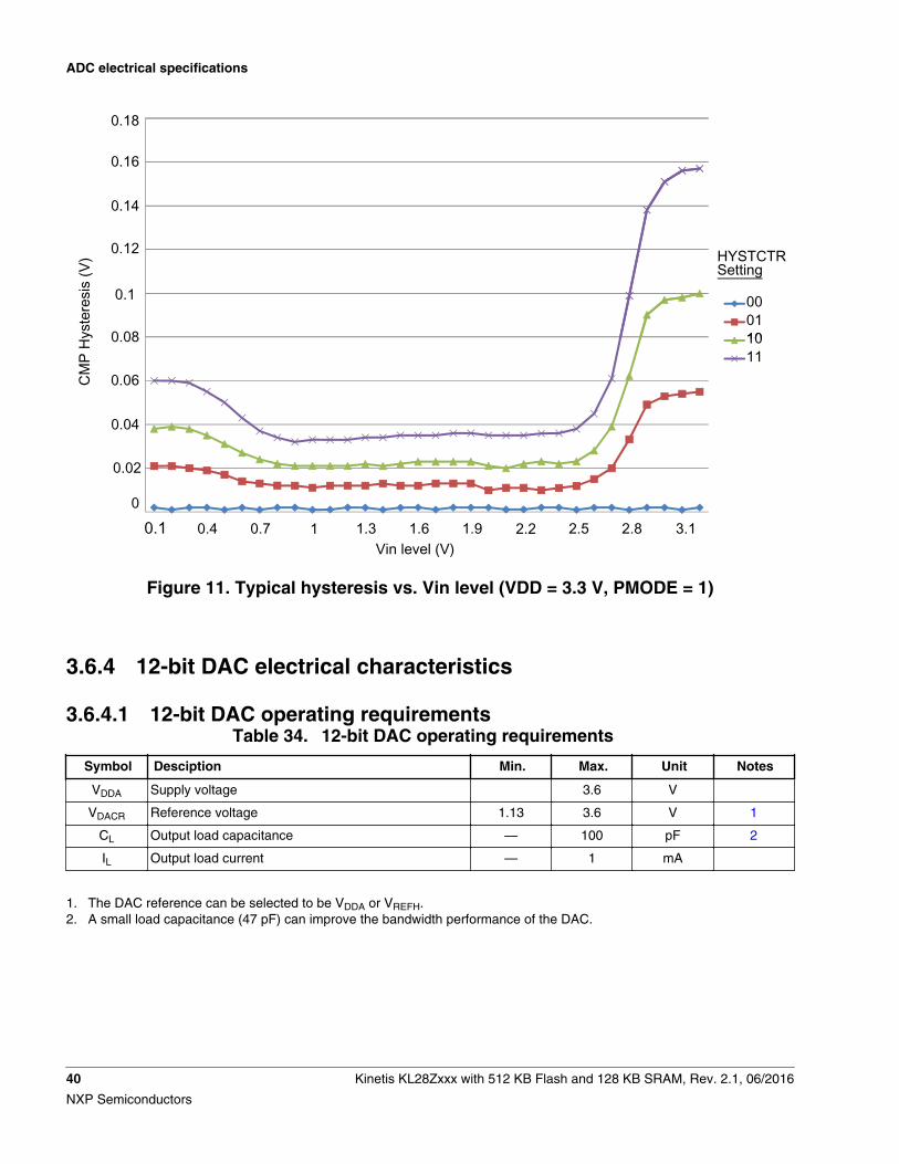
000110
HYSTCTR Setting
1011
0.1 3.12.82.52.21.91.61.310.70.4
0.1
0
0.02
0.04
0.06
0.18
0.14
0.12
0.08
0.16
Vin level (V)
CM
P H
yste
resi
s (V
)
Figure 11. Typical hysteresis vs. Vin level (VDD = 3.3 V, PMODE = 1)
3.6.4 12-bit DAC electrical characteristics
3.6.4.1 12-bit DAC operating requirementsTable 34. 12-bit DAC operating requirements
Symbol Desciption Min. Max. Unit Notes
VDDA Supply voltage 3.6 V
VDACR Reference voltage 1.13 3.6 V 1
CL Output load capacitance — 100 pF 2
IL Output load current — 1 mA
1. The DAC reference can be selected to be VDDA or VREFH.2. A small load capacitance (47 pF) can improve the bandwidth performance of the DAC.
ADC electrical specifications
40 Kinetis KL28Zxxx with 512 KB Flash and 128 KB SRAM, Rev. 2.1, 06/2016
NXP Semiconductors
3.6.4.2 12-bit DAC operating behaviorsTable 35. 12-bit DAC operating behaviors
Symbol Description Min. Typ. Max. Unit Notes
IDDA_DACL
P
Supply current — low-power mode — — 250 μA
IDDA_DACH
P
Supply current — high-speed mode — — 900 μA
tDACLP Full-scale settling time (0x080 to 0xF7F) —low-power mode
— 100 200 μs 1
tDACHP Full-scale settling time (0x080 to 0xF7F) —high-power mode
— 15 30 μs 1
tCCDACLP Code-to-code settling time (0xBF8 to0xC08) — low-power mode and high-speed mode
— 0.7 1 μs 1
Vdacoutl DAC output voltage range low — high-speed mode, no load, DAC set to 0x000
— — 100 mV
Vdacouth DAC output voltage range high — high-speed mode, no load, DAC set to 0xFFF
VDACR−100
— VDACR mV
INL Integral non-linearity error — high speedmode
— — ±8 LSB 2
DNL Differential non-linearity error — VDACR > 2V
— — ±1 LSB 3
DNL Differential non-linearity error — VDACR =VREF_OUT
— — ±1 LSB 4
VOFFSET Offset error — ±0.4 ±0.8 %FSR 5
EG Gain error — ±0.1 ±0.6 %FSR 5
PSRR Power supply rejection ratio, VDDA ≥ 2.4 V 60 — 90 dB
TCO Temperature coefficient offset voltage — 3.7 — μV/C 6
TGE Temperature coefficient gain error — 0.000421 — %FSR/C
Rop Output resistance (load = 3 kΩ) — — 250 Ω
SR Slew rate -80h→ F7Fh→ 80h
• High power (SPHP)
• Low power (SPLP)
1.2
0.05
1.7
0.12
—
—
V/μs
BW 3dB bandwidth
• High power (SPHP)
• Low power (SPLP)
550
40
—
—
—
—
kHz
1. Settling within ±1 LSB2. The INL is measured for 0 + 100 mV to VDACR −100 mV3. The DNL is measured for 0 + 100 mV to VDACR −100 mV4. The DNL is measured for 0 + 100 mV to VDACR −100 mV with VDDA > 2.4 V5. Calculated by a best fit curve from VSS + 100 mV to VDACR − 100 mV6. VDDA = 3.0 V, reference select set for VDDA (DACx_CO:DACRFS = 1), high power mode (DACx_C0:LPEN = 0), DAC
set to 0x800, temperature range is across the full range of the device
ADC electrical specifications
Kinetis KL28Zxxx with 512 KB Flash and 128 KB SRAM, Rev. 2.1, 06/2016 41
NXP Semiconductors
Digital Code
DAC
12 IN
L (L
SB)
0
500 1000 1500 2000 2500 3000 3500 4000
2
4
6
8
-2
-4
-6
-80
Figure 12. Typical INL error vs. digital code
ADC electrical specifications
42 Kinetis KL28Zxxx with 512 KB Flash and 128 KB SRAM, Rev. 2.1, 06/2016
NXP Semiconductors
Temperature °C
DAC
12 M
id L
evel
Cod
e Vo
ltage
25 55 85 105 125
1.499
-40
1.4985
1.498
1.4975
1.497
1.4965
1.496
Figure 13. Offset at half scale vs. temperature
3.7 Timers
See General switching specifications.
3.8 Communication interfaces
3.8.1 EMV SIM specifications
Each EMV SIM module interface consists of a total of five pins.
ADC electrical specifications
Kinetis KL28Zxxx with 512 KB Flash and 128 KB SRAM, Rev. 2.1, 06/2016 43
NXP Semiconductors
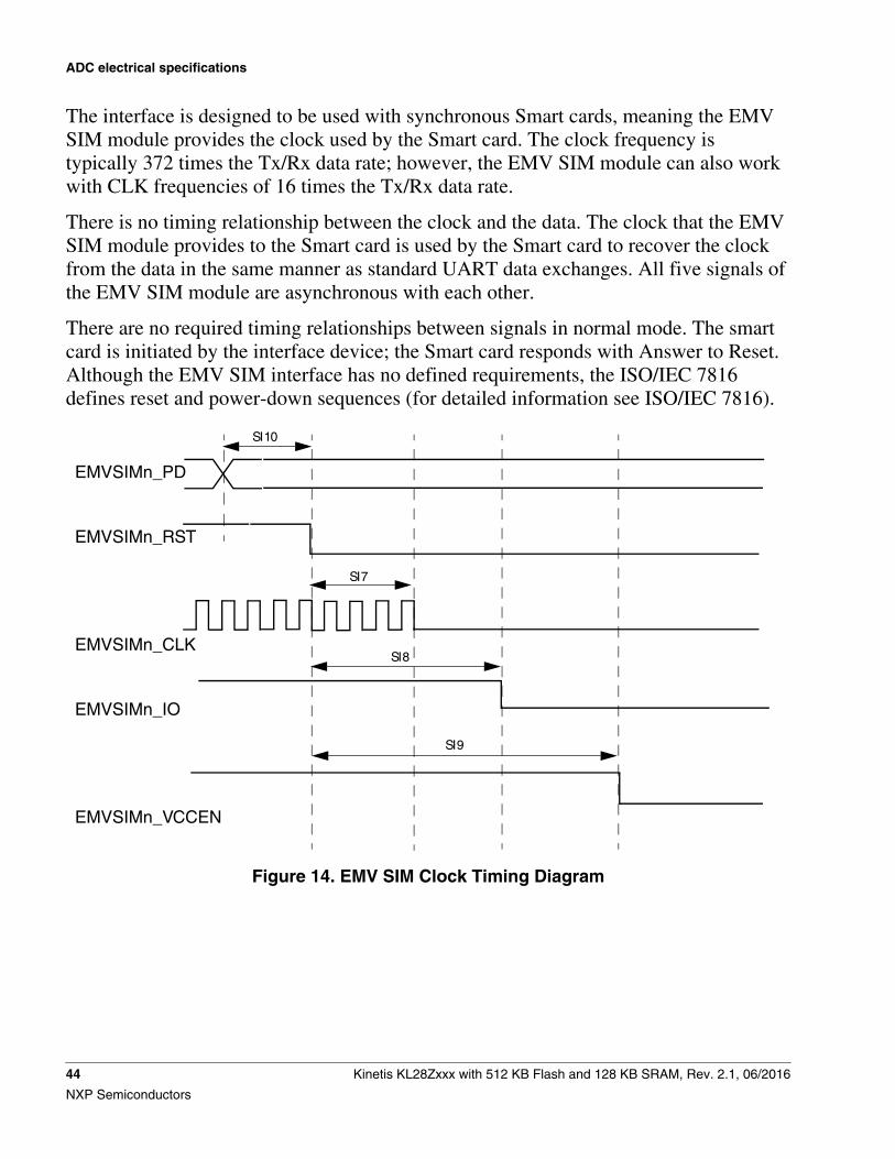
The interface is designed to be used with synchronous Smart cards, meaning the EMVSIM module provides the clock used by the Smart card. The clock frequency istypically 372 times the Tx/Rx data rate; however, the EMV SIM module can also workwith CLK frequencies of 16 times the Tx/Rx data rate.
There is no timing relationship between the clock and the data. The clock that the EMVSIM module provides to the Smart card is used by the Smart card to recover the clockfrom the data in the same manner as standard UART data exchanges. All five signals ofthe EMV SIM module are asynchronous with each other.
There are no required timing relationships between signals in normal mode. The smartcard is initiated by the interface device; the Smart card responds with Answer to Reset.Although the EMV SIM interface has no defined requirements, the ISO/IEC 7816defines reset and power-down sequences (for detailed information see ISO/IEC 7816).
EMVSIMn_PD
EMVSIMn_RST
EMVSIMn_CLK
EMVSIMn_IO
EMVSIMn_VCCEN
SI7
SI8
SI9
SI10
Figure 14. EMV SIM Clock Timing Diagram
ADC electrical specifications
44 Kinetis KL28Zxxx with 512 KB Flash and 128 KB SRAM, Rev. 2.1, 06/2016
NXP Semiconductors
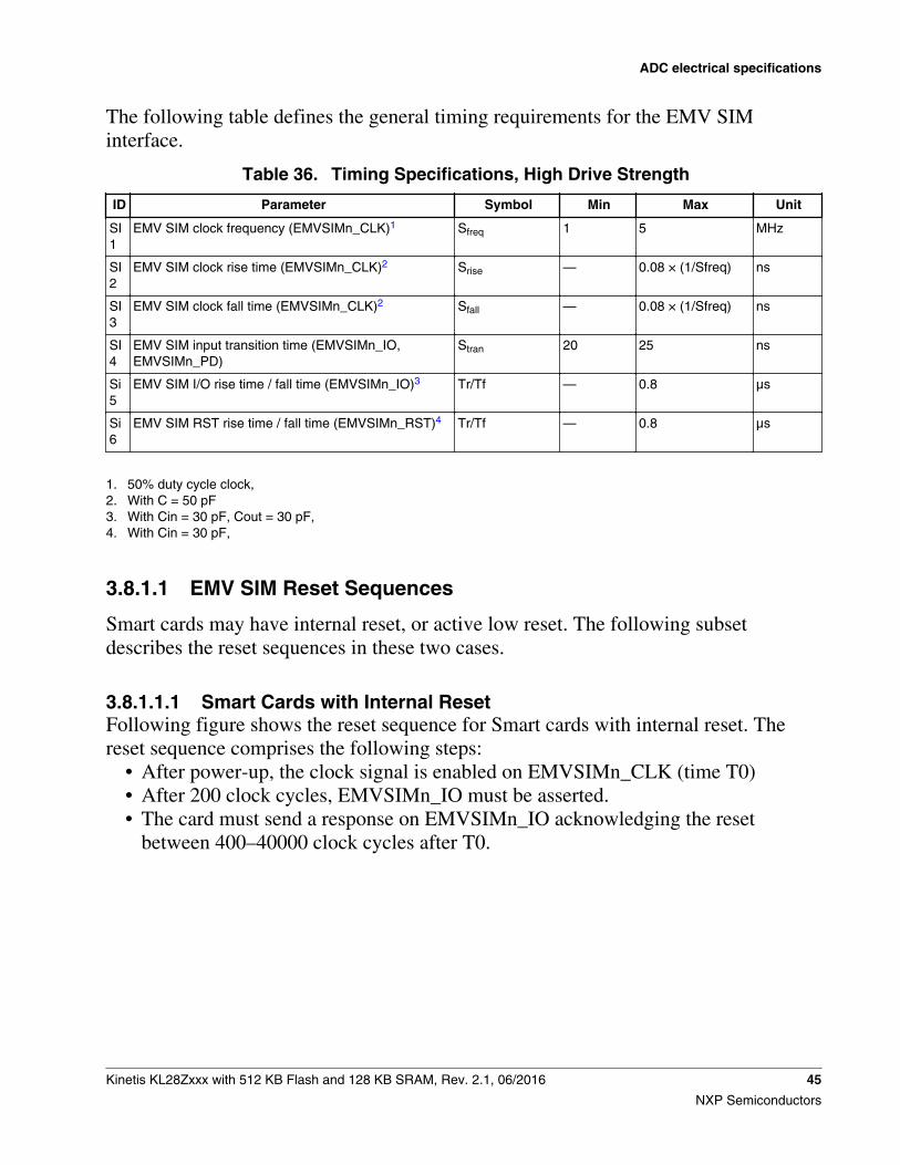
The following table defines the general timing requirements for the EMV SIMinterface.
Table 36. Timing Specifications, High Drive Strength
ID Parameter Symbol Min Max Unit
SI1
EMV SIM clock frequency (EMVSIMn_CLK)1 Sfreq 1 5 MHz
SI2
EMV SIM clock rise time (EMVSIMn_CLK)2 Srise — 0.08 × (1/Sfreq) ns
SI3
EMV SIM clock fall time (EMVSIMn_CLK)2 Sfall — 0.08 × (1/Sfreq) ns
SI4
EMV SIM input transition time (EMVSIMn_IO,EMVSIMn_PD)
Stran 20 25 ns
Si5
EMV SIM I/O rise time / fall time (EMVSIMn_IO)3 Tr/Tf — 0.8 μs
Si6
EMV SIM RST rise time / fall time (EMVSIMn_RST)4 Tr/Tf — 0.8 μs
1. 50% duty cycle clock,2. With C = 50 pF3. With Cin = 30 pF, Cout = 30 pF,4. With Cin = 30 pF,
3.8.1.1 EMV SIM Reset Sequences
Smart cards may have internal reset, or active low reset. The following subsetdescribes the reset sequences in these two cases.
3.8.1.1.1 Smart Cards with Internal ResetFollowing figure shows the reset sequence for Smart cards with internal reset. Thereset sequence comprises the following steps:
• After power-up, the clock signal is enabled on EMVSIMn_CLK (time T0)• After 200 clock cycles, EMVSIMn_IO must be asserted.• The card must send a response on EMVSIMn_IO acknowledging the reset
between 400–40000 clock cycles after T0.
ADC electrical specifications
Kinetis KL28Zxxx with 512 KB Flash and 128 KB SRAM, Rev. 2.1, 06/2016 45
NXP Semiconductors
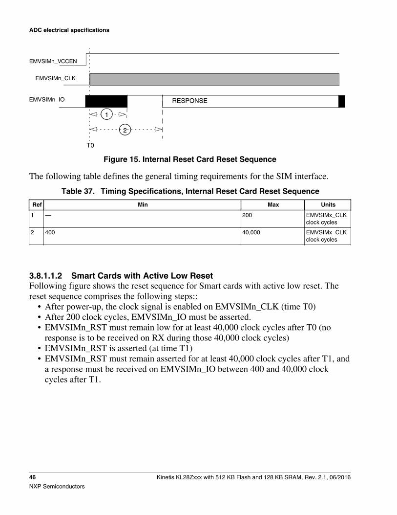
EMVSIMn_CLK
EMVSIMn_IO
2
T0
RESPONSE
1
EMVSIMn_VCCEN
Figure 15. Internal Reset Card Reset Sequence
The following table defines the general timing requirements for the SIM interface.
Table 37. Timing Specifications, Internal Reset Card Reset Sequence
Ref Min Max Units
1 — 200 EMVSIMx_CLKclock cycles
2 400 40,000 EMVSIMx_CLKclock cycles
3.8.1.1.2 Smart Cards with Active Low ResetFollowing figure shows the reset sequence for Smart cards with active low reset. Thereset sequence comprises the following steps::
• After power-up, the clock signal is enabled on EMVSIMn_CLK (time T0)• After 200 clock cycles, EMVSIMn_IO must be asserted.• EMVSIMn_RST must remain low for at least 40,000 clock cycles after T0 (no
response is to be received on RX during those 40,000 clock cycles)• EMVSIMn_RST is asserted (at time T1)• EMVSIMn_RST must remain asserted for at least 40,000 clock cycles after T1, and
a response must be received on EMVSIMn_IO between 400 and 40,000 clockcycles after T1.
ADC electrical specifications
46 Kinetis KL28Zxxx with 512 KB Flash and 128 KB SRAM, Rev. 2.1, 06/2016
NXP Semiconductors
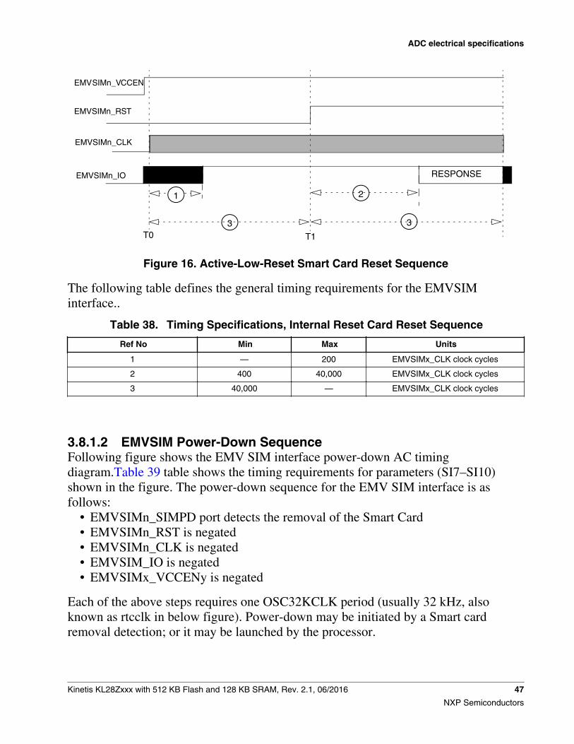
EMVSIMn_VCCEN
EMVSIMn_CLK
EMVSIMn_IO
2
T0
1 RESPONSE
EMVSIMn_RST
T1
33
Figure 16. Active-Low-Reset Smart Card Reset Sequence
The following table defines the general timing requirements for the EMVSIMinterface..
Table 38. Timing Specifications, Internal Reset Card Reset Sequence
Ref No Min Max Units
1 — 200 EMVSIMx_CLK clock cycles
2 400 40,000 EMVSIMx_CLK clock cycles
3 40,000 — EMVSIMx_CLK clock cycles
3.8.1.2 EMVSIM Power-Down SequenceFollowing figure shows the EMV SIM interface power-down AC timingdiagram.Table 39 table shows the timing requirements for parameters (SI7–SI10)shown in the figure. The power-down sequence for the EMV SIM interface is asfollows:
• EMVSIMn_SIMPD port detects the removal of the Smart Card• EMVSIMn_RST is negated• EMVSIMn_CLK is negated• EMVSIM_IO is negated• EMVSIMx_VCCENy is negated
Each of the above steps requires one OSC32KCLK period (usually 32 kHz, alsoknown as rtcclk in below figure). Power-down may be initiated by a Smart cardremoval detection; or it may be launched by the processor.
ADC electrical specifications
Kinetis KL28Zxxx with 512 KB Flash and 128 KB SRAM, Rev. 2.1, 06/2016 47
NXP Semiconductors

EMVSIMn_PD
EMVSIMn_RST
EMVSIMn_CLK
EMVSIMn_IO
EMVSIMn_VCCEN
SI7
SI8
SI9
SI10
Figure 17. Smart Card Interface Power Down AC Timing
Table 39. Timing Requirements for Power-down Sequence
Ref No Parameter Symbol Min Max Units
SI7 EMVSIM reset to SIM clock stop Srst2clk 0.9 × 1/Frtcclk1
1.1 × 1/Frtcclk μs
SI8 EMVSIM reset to SIM Tx datalow
Srst2dat 1.8 × 1/Frtcclk 2.2 × 1/Frtcclk μs
SI9 EMVSIM reset to SIM voltageenable low
Srst2ven 2.7 × 1/Frtcclk 3.3 × 1/Frtcclk μs
SI10 EMVSIM presence detect to SIMreset low
Spd2rst 0.9 × 1/Frtcclk 1.1 × 1/Frtcclk μs
1. Frtcclk is OSC32KCLK, and this clock must be enabled during the power down sequence.
NOTESame timing is also followed when auto power down isinitiated. See Reference Manual for reference.
ADC electrical specifications
48 Kinetis KL28Zxxx with 512 KB Flash and 128 KB SRAM, Rev. 2.1, 06/2016
NXP Semiconductors
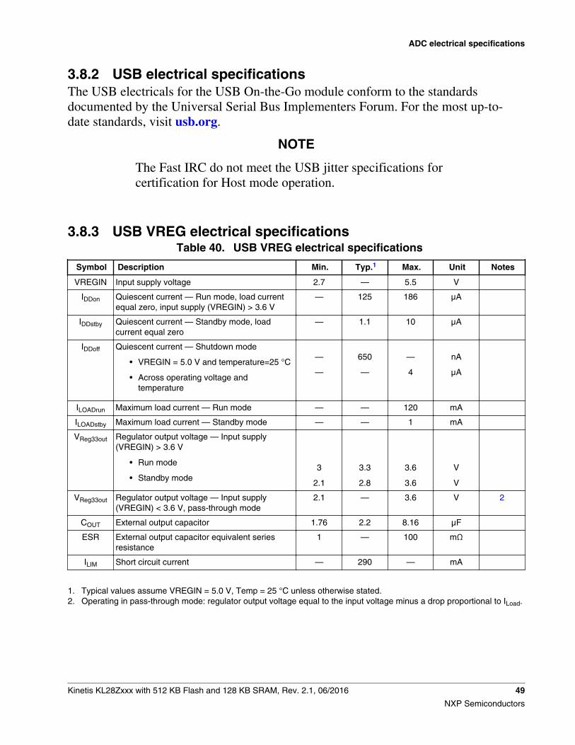
3.8.2 USB electrical specificationsThe USB electricals for the USB On-the-Go module conform to the standardsdocumented by the Universal Serial Bus Implementers Forum. For the most up-to-date standards, visit usb.org.
NOTE
The Fast IRC do not meet the USB jitter specifications forcertification for Host mode operation.
3.8.3 USB VREG electrical specificationsTable 40. USB VREG electrical specifications
Symbol Description Min. Typ.1 Max. Unit Notes
VREGIN Input supply voltage 2.7 — 5.5 V
IDDon Quiescent current — Run mode, load currentequal zero, input supply (VREGIN) > 3.6 V
— 125 186 μA
IDDstby Quiescent current — Standby mode, loadcurrent equal zero
— 1.1 10 μA
IDDoff Quiescent current — Shutdown mode
• VREGIN = 5.0 V and temperature=25 °C
• Across operating voltage andtemperature
—
—
650
—
—
4
nA
μA
ILOADrun Maximum load current — Run mode — — 120 mA
ILOADstby Maximum load current — Standby mode — — 1 mA
VReg33out Regulator output voltage — Input supply(VREGIN) > 3.6 V
• Run mode
• Standby mode
3
2.1
3.3
2.8
3.6
3.6
V
V
VReg33out Regulator output voltage — Input supply(VREGIN) < 3.6 V, pass-through mode
2.1 — 3.6 V 2
COUT External output capacitor 1.76 2.2 8.16 μF
ESR External output capacitor equivalent seriesresistance
1 — 100 mΩ
ILIM Short circuit current — 290 — mA
1. Typical values assume VREGIN = 5.0 V, Temp = 25 °C unless otherwise stated.2. Operating in pass-through mode: regulator output voltage equal to the input voltage minus a drop proportional to ILoad.
ADC electrical specifications
Kinetis KL28Zxxx with 512 KB Flash and 128 KB SRAM, Rev. 2.1, 06/2016 49
NXP Semiconductors
3.8.4 LPSPI switching specifications
The Low Power Serial Peripheral Interface (LPSPI) provides a synchronous serial buswith master and slave operations. Many of the transfer attributes are programmable.The following tables provide timing characteristics for classic SPI timing modes.
All timing is shown with respect to 20% VDD and 80% VDD thresholds, unless noted, aswell as input signal transitions of 3 ns and a 30 pF maximum load on all LPSPI pins.
NOTE• Slew rate disabled pads are those pins with
PORTx_PCRn[SRE] bit cleared. Slew rate enabled padsare those pins with PORTx_PCRn[SRE] bit set.
• To achieve high bit rate, it is recommended to use fastpins (PTE20, PTE21, PTE22, PTE23, PTD4, PTD5,PTD6, and PTD7) and/or high drive pins (PTC3, PTC4,PTD4, PTD5, PTD6, and PTD7).
Table 41. LPSPI master mode timing on slew rate disabled pads
Num. Symbol Description Min. Max. Unit Note
1 fop Frequency of operation fperiph/2048 fperiph/2 Hz 1
2 tSPSCK SPSCK period 2 x tperiph 2048 xtperiph
ns 2
3 tLead Enable lead time 1/2 — tSPSCK —
4 tLag Enable lag time 1/2 — tSPSCK —
5 tWSPSCK Clock (SPSCK) high or low time tperiph - 30 1024 xtperiph
ns —
6 tSU Data setup time (inputs) 18 — ns —
7 tHI Data hold time (inputs) 0 — ns —
8 tv Data valid (after SPSCK edge) — 15 ns —
9 tHO Data hold time (outputs) 0 — ns —
10 tRI Rise time input — tperiph - 25 ns —
tFI Fall time input
11 tRO Rise time output — 25 ns —
tFO Fall time output
1. fperiph is the LPSPI peripheral functional clock.2. tperiph = 1/fperiph
Table 42. LPSPI master mode timing on slew rate enabled pads
Num. Symbol Description Min. Max. Unit Note
1 fop Frequency of operation fperiph/2048 fperiph/2 Hz 1
Table continues on the next page...
ADC electrical specifications
50 Kinetis KL28Zxxx with 512 KB Flash and 128 KB SRAM, Rev. 2.1, 06/2016
NXP Semiconductors
Table 42. LPSPI master mode timing on slew rate enabled pads (continued)
Num. Symbol Description Min. Max. Unit Note
2 tSPSCK SPSCK period 2 x tperiph 2048 xtperiph
ns 2
3 tLead Enable lead time 1/2 — tSPSCK —
4 tLag Enable lag time 1/2 — tSPSCK —
5 tWSPSCK Clock (SPSCK) high or low time tperiph - 30 1024 xtperiph
ns —
6 tSU Data setup time (inputs) 96 — ns —
7 tHI Data hold time (inputs) 0 — ns —
8 tv Data valid (after SPSCK edge) — 52 ns —
9 tHO Data hold time (outputs) 0 — ns —
10 tRI Rise time input — tperiph - 25 ns —
tFI Fall time input
11 tRO Rise time output — 36 ns —
tFO Fall time output
1. fperiph is the LPSPI peripheral functional clock2. tperiph = 1/fperiph
(OUTPUT)
2
8
6 7
MSB IN2 LSB IN
MSB OUT2 LSB OUT
9
5
5
3
(CPOL=0)
411
1110
10SPSCK
SPSCK(CPOL=1)
2. LSBF = 0. For LSBF = 1, bit order is LSB, bit 1, ..., bit 6, MSB.1. If configured as an output.
SS1
(OUTPUT)
(OUTPUT)
MOSI(OUTPUT)
MISO(INPUT) BIT 6 . . . 1
BIT 6 . . . 1
Figure 18. LPSPI master mode timing (CPHA = 0)
ADC electrical specifications
Kinetis KL28Zxxx with 512 KB Flash and 128 KB SRAM, Rev. 2.1, 06/2016 51
NXP Semiconductors
<<CLASSIFICATION>> <<NDA MESSAGE>>
38
2
6 7
MSB IN2
BIT 6 . . . 1 MASTER MSB OUT2 MASTER LSB OUT
55
8
10 11
PORT DATA PORT DATA
3 10 11 4
1.If configured as output 2. LSBF = 0. For LSBF = 1, bit order is LSB, bit 1, ..., bit 6, MSB.
9
(OUTPUT)
(CPOL=0)SPSCK
SPSCK(CPOL=1)
SS1
(OUTPUT)
(OUTPUT)
MOSI(OUTPUT)
MISO(INPUT) LSB INBIT 6 . . . 1
Figure 19. LPSPI master mode timing (CPHA = 1)
Table 43. LPSPI slave mode timing on slew rate disabled pads
Num. Symbol Description Min. Max. Unit Note
1 fop Frequency of operation 0 fperiph/4 Hz 1
2 tSPSCK SPSCK period 4 x tperiph — ns 2
3 tLead Enable lead time 1 — tperiph —
4 tLag Enable lag time 1 — tperiph —
5 tWSPSCK Clock (SPSCK) high or low time tperiph - 30 — ns —
6 tSU Data setup time (inputs) 2.5 — ns —
7 tHI Data hold time (inputs) 3.5 — ns —
8 ta Slave access time — tperiph ns 3
9 tdis Slave MISO disable time — tperiph ns 4
10 tv Data valid (after SPSCK edge) — 31 ns —
11 tHO Data hold time (outputs) 0 — ns —
12 tRI Rise time input — tperiph - 25 ns —
tFI Fall time input
13 tRO Rise time output — 25 ns —
tFO Fall time output
1. fperiph is the LPSPI peripheral functional clock2. tperiph = 1/fperiph3. Time to data active from high-impedance state4. Hold time to high-impedance state
ADC electrical specifications
52 Kinetis KL28Zxxx with 512 KB Flash and 128 KB SRAM, Rev. 2.1, 06/2016
NXP Semiconductors
Table 44. LPSPI slave mode timing on slew rate enabled pads
Num. Symbol Description Min. Max. Unit Note
1 fop Frequency of operation 0 fperiph/4 Hz 1
2 tSPSCK SPSCK period 4 x tperiph — ns 2
3 tLead Enable lead time 1 — tperiph —
4 tLag Enable lag time 1 — tperiph —
5 tWSPSCK Clock (SPSCK) high or low time tperiph - 30 — ns —
6 tSU Data setup time (inputs) 2 — ns —
7 tHI Data hold time (inputs) 7 — ns —
8 ta Slave access time — tperiph ns 3
9 tdis Slave MISO disable time — tperiph ns 4
10 tv Data valid (after SPSCK edge) — 122 ns —
11 tHO Data hold time (outputs) 0 — ns —
12 tRI Rise time input — tperiph - 25 ns —
tFI Fall time input
13 tRO Rise time output — 36 ns —
tFO Fall time output
1. fperiph is the LPSPI peripheral functional clock2. tperiph = 1/fperiph3. Time to data active from high-impedance state4. Hold time to high-impedance state
2
10
6 7
MSB IN
BIT 6 . . . 1 SLAVE MSB SLAVE LSB OUT
11
553
8
4
13
NOTE: Not defined
12
12
11
SEE NOTE
13
9
see note
(INPUT)
(CPOL=0)SPSCK
SPSCK(CPOL=1)
SS
(INPUT)
(INPUT)
MOSI(INPUT)
MISO(OUTPUT)
LSB INBIT 6 . . . 1
Figure 20. LPSPI slave mode timing (CPHA = 0)
ADC electrical specifications
Kinetis KL28Zxxx with 512 KB Flash and 128 KB SRAM, Rev. 2.1, 06/2016 53
NXP Semiconductors
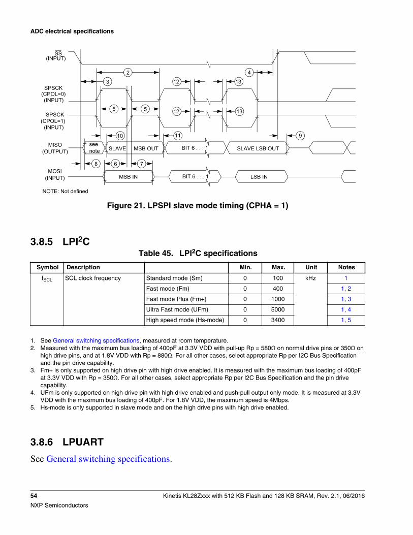
2
6 7
MSB IN
BIT 6 . . . 1 MSB OUT SLAVE LSB OUT
55
10
12 13
3 12 134
SLAVE
8
9see note
(INPUT)
(CPOL=0)SPSCK
SPSCK(CPOL=1)
SS
(INPUT)
(INPUT)
MOSI(INPUT)
MISO(OUTPUT)
NOTE: Not defined
11
LSB INBIT 6 . . . 1
Figure 21. LPSPI slave mode timing (CPHA = 1)
3.8.5 LPI2CTable 45. LPI2C specifications
Symbol Description Min. Max. Unit Notes
fSCL SCL clock frequency Standard mode (Sm) 0 100 kHz 1
Fast mode (Fm) 0 400 1, 2
Fast mode Plus (Fm+) 0 1000 1, 3
Ultra Fast mode (UFm) 0 5000 1, 4
High speed mode (Hs-mode) 0 3400 1, 5
1. See General switching specifications, measured at room temperature.2. Measured with the maximum bus loading of 400pF at 3.3V VDD with pull-up Rp = 580Ω on normal drive pins or 350Ω on
high drive pins, and at 1.8V VDD with Rp = 880Ω. For all other cases, select appropriate Rp per I2C Bus Specificationand the pin drive capability.
3. Fm+ is only supported on high drive pin with high drive enabled. It is measured with the maximum bus loading of 400pFat 3.3V VDD with Rp = 350Ω. For all other cases, select appropriate Rp per I2C Bus Specification and the pin drivecapability.
4. UFm is only supported on high drive pin with high drive enabled and push-pull output only mode. It is measured at 3.3VVDD with the maximum bus loading of 400pF. For 1.8V VDD, the maximum speed is 4Mbps.
5. Hs-mode is only supported in slave mode and on the high drive pins with high drive enabled.
3.8.6 LPUART
See General switching specifications.
ADC electrical specifications
54 Kinetis KL28Zxxx with 512 KB Flash and 128 KB SRAM, Rev. 2.1, 06/2016
NXP Semiconductors
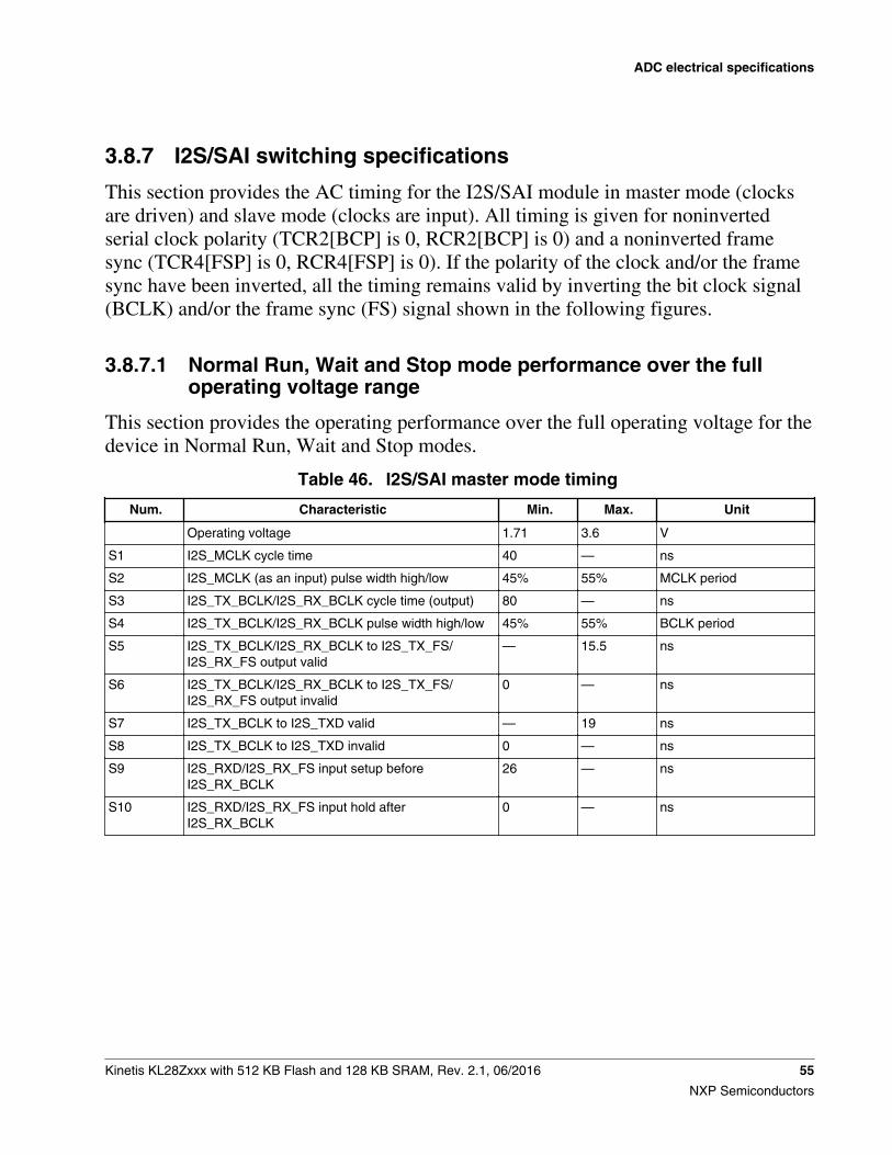
3.8.7 I2S/SAI switching specifications
This section provides the AC timing for the I2S/SAI module in master mode (clocksare driven) and slave mode (clocks are input). All timing is given for noninvertedserial clock polarity (TCR2[BCP] is 0, RCR2[BCP] is 0) and a noninverted framesync (TCR4[FSP] is 0, RCR4[FSP] is 0). If the polarity of the clock and/or the framesync have been inverted, all the timing remains valid by inverting the bit clock signal(BCLK) and/or the frame sync (FS) signal shown in the following figures.
3.8.7.1 Normal Run, Wait and Stop mode performance over the fulloperating voltage range
This section provides the operating performance over the full operating voltage for thedevice in Normal Run, Wait and Stop modes.
Table 46. I2S/SAI master mode timing
Num. Characteristic Min. Max. Unit
Operating voltage 1.71 3.6 V
S1 I2S_MCLK cycle time 40 — ns
S2 I2S_MCLK (as an input) pulse width high/low 45% 55% MCLK period
S3 I2S_TX_BCLK/I2S_RX_BCLK cycle time (output) 80 — ns
S4 I2S_TX_BCLK/I2S_RX_BCLK pulse width high/low 45% 55% BCLK period
S5 I2S_TX_BCLK/I2S_RX_BCLK to I2S_TX_FS/I2S_RX_FS output valid
— 15.5 ns
S6 I2S_TX_BCLK/I2S_RX_BCLK to I2S_TX_FS/I2S_RX_FS output invalid
0 — ns
S7 I2S_TX_BCLK to I2S_TXD valid — 19 ns
S8 I2S_TX_BCLK to I2S_TXD invalid 0 — ns
S9 I2S_RXD/I2S_RX_FS input setup beforeI2S_RX_BCLK
26 — ns
S10 I2S_RXD/I2S_RX_FS input hold afterI2S_RX_BCLK
0 — ns
ADC electrical specifications
Kinetis KL28Zxxx with 512 KB Flash and 128 KB SRAM, Rev. 2.1, 06/2016 55
NXP Semiconductors
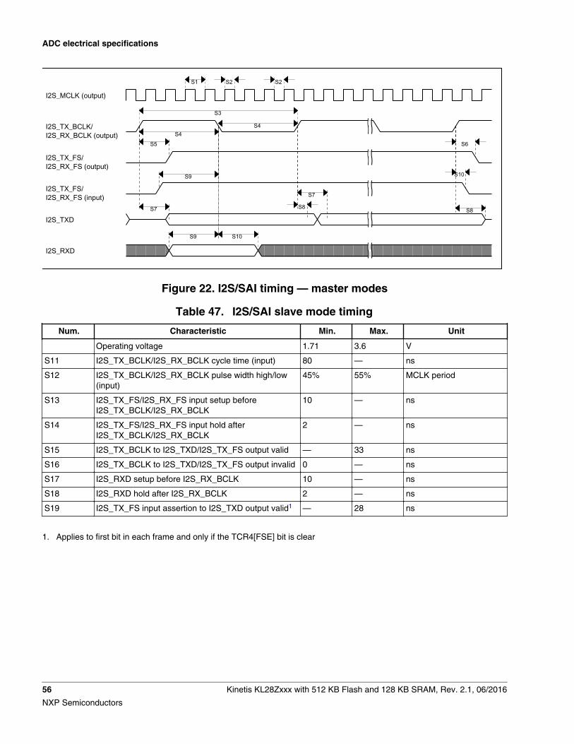
S1 S2 S2
S3
S4S4
S5
S9
S7
S9 S10
S7
S8
S6
S10
S8
I2S_MCLK (output)
I2S_TX_BCLK/ I2S_RX_BCLK (output)
I2S_TX_FS/ I2S_RX_FS (output)
I2S_TX_FS/ I2S_RX_FS (input)
I2S_TXD
I2S_RXD
Figure 22. I2S/SAI timing — master modes
Table 47. I2S/SAI slave mode timing
Num. Characteristic Min. Max. Unit
Operating voltage 1.71 3.6 V
S11 I2S_TX_BCLK/I2S_RX_BCLK cycle time (input) 80 — ns
S12 I2S_TX_BCLK/I2S_RX_BCLK pulse width high/low(input)
45% 55% MCLK period
S13 I2S_TX_FS/I2S_RX_FS input setup beforeI2S_TX_BCLK/I2S_RX_BCLK
10 — ns
S14 I2S_TX_FS/I2S_RX_FS input hold afterI2S_TX_BCLK/I2S_RX_BCLK
2 — ns
S15 I2S_TX_BCLK to I2S_TXD/I2S_TX_FS output valid — 33 ns
S16 I2S_TX_BCLK to I2S_TXD/I2S_TX_FS output invalid 0 — ns
S17 I2S_RXD setup before I2S_RX_BCLK 10 — ns
S18 I2S_RXD hold after I2S_RX_BCLK 2 — ns
S19 I2S_TX_FS input assertion to I2S_TXD output valid1 — 28 ns
1. Applies to first bit in each frame and only if the TCR4[FSE] bit is clear
ADC electrical specifications
56 Kinetis KL28Zxxx with 512 KB Flash and 128 KB SRAM, Rev. 2.1, 06/2016
NXP Semiconductors
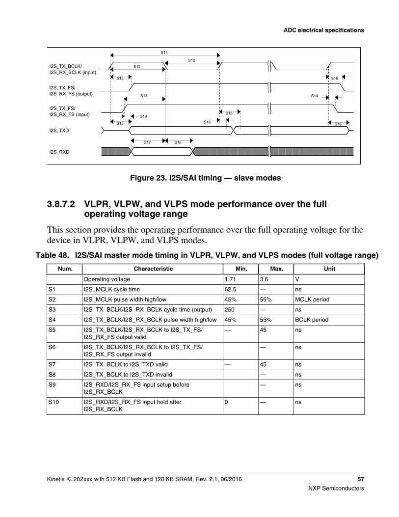
S15
S13
S15
S17 S18
S15
S16
S16
S14
S16
S11
S12S12
I2S_TX_BCLK/ I2S_RX_BCLK (input)
I2S_TX_FS/ I2S_RX_FS (output)
I2S_TXD
I2S_RXD
I2S_TX_FS/ I2S_RX_FS (input) S19
Figure 23. I2S/SAI timing — slave modes
3.8.7.2 VLPR, VLPW, and VLPS mode performance over the fulloperating voltage range
This section provides the operating performance over the full operating voltage for thedevice in VLPR, VLPW, and VLPS modes.
Table 48. I2S/SAI master mode timing in VLPR, VLPW, and VLPS modes (full voltage range)
Num. Characteristic Min. Max. Unit
Operating voltage 1.71 3.6 V
S1 I2S_MCLK cycle time 62.5 — ns
S2 I2S_MCLK pulse width high/low 45% 55% MCLK period
S3 I2S_TX_BCLK/I2S_RX_BCLK cycle time (output) 250 — ns
S4 I2S_TX_BCLK/I2S_RX_BCLK pulse width high/low 45% 55% BCLK period
S5 I2S_TX_BCLK/I2S_RX_BCLK to I2S_TX_FS/I2S_RX_FS output valid
— 45 ns
S6 I2S_TX_BCLK/I2S_RX_BCLK to I2S_TX_FS/I2S_RX_FS output invalid
— ns
S7 I2S_TX_BCLK to I2S_TXD valid — 45 ns
S8 I2S_TX_BCLK to I2S_TXD invalid — ns
S9 I2S_RXD/I2S_RX_FS input setup beforeI2S_RX_BCLK
— ns
S10 I2S_RXD/I2S_RX_FS input hold afterI2S_RX_BCLK
0 — ns
ADC electrical specifications
Kinetis KL28Zxxx with 512 KB Flash and 128 KB SRAM, Rev. 2.1, 06/2016 57
NXP Semiconductors

S1 S2 S2
S3
S4S4
S5
S9
S7
S9 S10
S7
S8
S6
S10
S8
I2S_MCLK (output)
I2S_TX_BCLK/ I2S_RX_BCLK (output)
I2S_TX_FS/ I2S_RX_FS (output)
I2S_TX_FS/ I2S_RX_FS (input)
I2S_TXD
I2S_RXD
Figure 24. I2S/SAI timing — master modes
Table 49. I2S/SAI slave mode timing in VLPR, VLPW, and VLPS modes (full voltage range)
Num. Characteristic Min. Max. Unit
Operating voltage 1.71 3.6 V
S11 I2S_TX_BCLK/I2S_RX_BCLK cycle time (input) 250 — ns
S12 I2S_TX_BCLK/I2S_RX_BCLK pulse width high/low(input)
45% 55% MCLK period
S13 I2S_TX_FS/I2S_RX_FS input setup beforeI2S_TX_BCLK/I2S_RX_BCLK
30 — ns
S14 I2S_TX_FS/I2S_RX_FS input hold afterI2S_TX_BCLK/I2S_RX_BCLK
— ns
S15 I2S_TX_BCLK to I2S_TXD/I2S_TX_FS output valid — ns
S16 I2S_TX_BCLK to I2S_TXD/I2S_TX_FS output invalid 0 — ns
S17 I2S_RXD setup before I2S_RX_BCLK 30 — ns
S18 I2S_RXD hold after I2S_RX_BCLK — ns
S19 I2S_TX_FS input assertion to I2S_TXD output valid1 — 72 ns
1. Applies to first bit in each frame and only if the TCR4[FSE] bit is clear
ADC electrical specifications
58 Kinetis KL28Zxxx with 512 KB Flash and 128 KB SRAM, Rev. 2.1, 06/2016
NXP Semiconductors
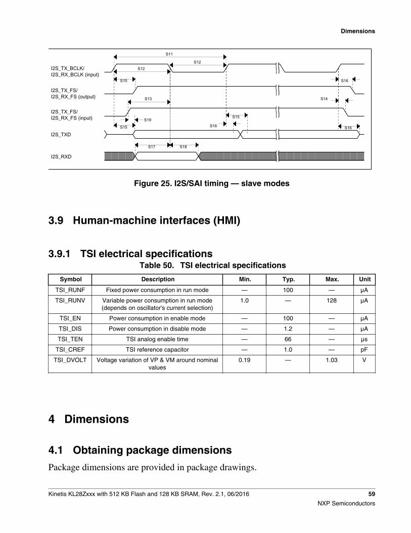
S15
S13
S15
S17 S18
S15
S16
S16
S14
S16
S11
S12S12
I2S_TX_BCLK/ I2S_RX_BCLK (input)
I2S_TX_FS/ I2S_RX_FS (output)
I2S_TXD
I2S_RXD
I2S_TX_FS/ I2S_RX_FS (input) S19
Figure 25. I2S/SAI timing — slave modes
3.9 Human-machine interfaces (HMI)
3.9.1 TSI electrical specificationsTable 50. TSI electrical specifications
Symbol Description Min. Typ. Max. Unit
TSI_RUNF Fixed power consumption in run mode — 100 — µA
TSI_RUNV Variable power consumption in run mode(depends on oscillator's current selection)
1.0 — 128 µA
TSI_EN Power consumption in enable mode — 100 — µA
TSI_DIS Power consumption in disable mode — 1.2 — µA
TSI_TEN TSI analog enable time — 66 — µs
TSI_CREF TSI reference capacitor — 1.0 — pF
TSI_DVOLT Voltage variation of VP & VM around nominalvalues
0.19 — 1.03 V
4 Dimensions
4.1 Obtaining package dimensions
Package dimensions are provided in package drawings.
Dimensions
Kinetis KL28Zxxx with 512 KB Flash and 128 KB SRAM, Rev. 2.1, 06/2016 59
NXP Semiconductors
To find a package drawing, go to nxp.com and perform a keyword search for thedrawing’s document number:
If you want the drawing for this package Then use this document number
100-pin LQFP 98ASS23308W
121-pin XFBGA 98ASA00595D
Pinouts and Packaging
5.1 KL28Z Signal Multiplexing and Pin Assignments
The following table shows the signals available on each pin and the locations of thesepins on the devices supported by this document. The Port Control Module is responsiblefor selecting which ALT function is available on each pin.
NOTEThe 121-pin XFBGA package for this product is not yetavailable. However, it is included in a Package Your Wayprogram for Kinetis MCUs. Visit nxp.com/KPYW for moredetails.
NOTE• A pull-up resistor (typically 4.7 KΩ) must be connected to
the EMVSIM0_IO pin if this pin is configured as EMVSIM function.
• PTB0/1, PTC3/4, PTD4/5/6/7 have both high drive andnormal/low drive capability. PTD4, PTD5, PTD6, PTD7,PTE20, PTE21, PTE22, PTE23 are also fast pins. When ahigh bit rate is required on the communication interfacepins, it is recommended to use fast pins. In case of highbus loading, the high drive strength of high drive pinsmust be enabled by setting the correspondingPORTx_PCRn[DSE] bit.
• RESET_b pin is open drain with internal pullup deviceand passive analog filter when configured as RESET pin(default state after POR). When this pin is configured toother shared functions, the passive analog filter isdisabled.
5
Pinouts and Packaging
60 Kinetis KL28Zxxx with 512 KB Flash and 128 KB SRAM, Rev. 2.1, 06/2016
NXP Semiconductors
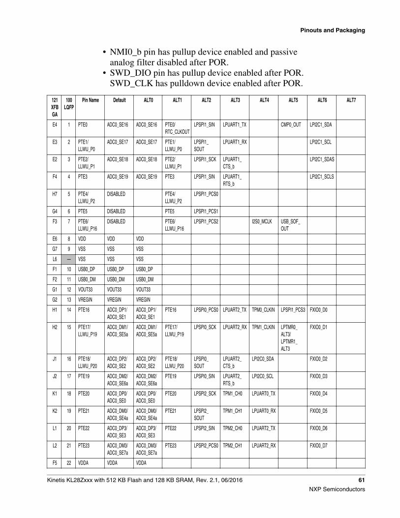
• NMI0_b pin has pullup device enabled and passiveanalog filter disabled after POR.
• SWD_DIO pin has pullup device enabled after POR.SWD_CLK has pulldown device enabled after POR.
121XFBGA
100LQFP
Pin Name Default ALT0 ALT1 ALT2 ALT3 ALT4 ALT5 ALT6 ALT7
E4 1 PTE0 ADC0_SE16 ADC0_SE16 PTE0/RTC_CLKOUT
LPSPI1_SIN LPUART1_TX CMP0_OUT LPI2C1_SDA
E3 2 PTE1/LLWU_P0
ADC0_SE17 ADC0_SE17 PTE1/LLWU_P0
LPSPI1_SOUT
LPUART1_RX LPI2C1_SCL
E2 3 PTE2/LLWU_P1
ADC0_SE18 ADC0_SE18 PTE2/LLWU_P1
LPSPI1_SCK LPUART1_CTS_b
LPI2C1_SDAS
F4 4 PTE3 ADC0_SE19 ADC0_SE19 PTE3 LPSPI1_SIN LPUART1_RTS_b
LPI2C1_SCLS
H7 5 PTE4/LLWU_P2
DISABLED PTE4/LLWU_P2
LPSPI1_PCS0
G4 6 PTE5 DISABLED PTE5 LPSPI1_PCS1
F3 7 PTE6/LLWU_P16
DISABLED PTE6/LLWU_P16
LPSPI1_PCS2 I2S0_MCLK USB_SOF_OUT
E6 8 VDD VDD VDD
G7 9 VSS VSS VSS
L6 — VSS VSS VSS
F1 10 USB0_DP USB0_DP USB0_DP
F2 11 USB0_DM USB0_DM USB0_DM
G1 12 VOUT33 VOUT33 VOUT33
G2 13 VREGIN VREGIN VREGIN
H1 14 PTE16 ADC0_DP1/ADC0_SE1
ADC0_DP1/ADC0_SE1
PTE16 LPSPI0_PCS0 LPUART2_TX TPM0_CLKIN LPSPI1_PCS3 FXIO0_D0
H2 15 PTE17/LLWU_P19
ADC0_DM1/ADC0_SE5a
ADC0_DM1/ADC0_SE5a
PTE17/LLWU_P19
LPSPI0_SCK LPUART2_RX TPM1_CLKIN LPTMR0_ALT3/LPTMR1_ALT3
FXIO0_D1
J1 16 PTE18/LLWU_P20
ADC0_DP2/ADC0_SE2
ADC0_DP2/ADC0_SE2
PTE18/LLWU_P20
LPSPI0_SOUT
LPUART2_CTS_b
LPI2C0_SDA FXIO0_D2
J2 17 PTE19 ADC0_DM2/ADC0_SE6a
ADC0_DM2/ADC0_SE6a
PTE19 LPSPI0_SIN LPUART2_RTS_b
LPI2C0_SCL FXIO0_D3
K1 18 PTE20 ADC0_DP0/ADC0_SE0
ADC0_DP0/ADC0_SE0
PTE20 LPSPI2_SCK TPM1_CH0 LPUART0_TX FXIO0_D4
K2 19 PTE21 ADC0_DM0/ADC0_SE4a
ADC0_DM0/ADC0_SE4a
PTE21 LPSPI2_SOUT
TPM1_CH1 LPUART0_RX FXIO0_D5
L1 20 PTE22 ADC0_DP3/ADC0_SE3
ADC0_DP3/ADC0_SE3
PTE22 LPSPI2_SIN TPM2_CH0 LPUART2_TX FXIO0_D6
L2 21 PTE23 ADC0_DM3/ADC0_SE7a
ADC0_DM3/ADC0_SE7a
PTE23 LPSPI2_PCS0 TPM2_CH1 LPUART2_RX FXIO0_D7
F5 22 VDDA VDDA VDDA
Pinouts and Packaging
Kinetis KL28Zxxx with 512 KB Flash and 128 KB SRAM, Rev. 2.1, 06/2016 61
NXP Semiconductors
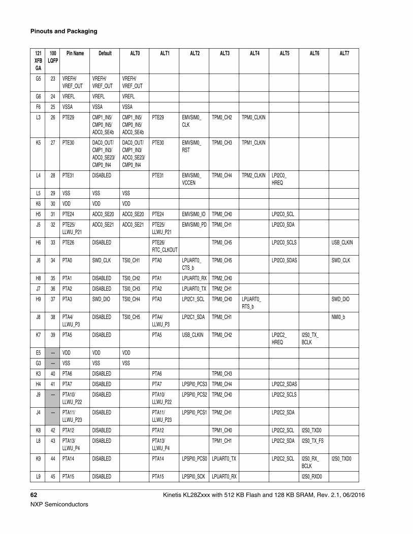
121XFBGA
100LQFP
Pin Name Default ALT0 ALT1 ALT2 ALT3 ALT4 ALT5 ALT6 ALT7
G5 23 VREFH/VREF_OUT
VREFH/VREF_OUT
VREFH/VREF_OUT
G6 24 VREFL VREFL VREFL
F6 25 VSSA VSSA VSSA
L3 26 PTE29 CMP1_IN5/CMP0_IN5/ADC0_SE4b
CMP1_IN5/CMP0_IN5/ADC0_SE4b
PTE29 EMVSIM0_CLK
TPM0_CH2 TPM0_CLKIN
K5 27 PTE30 DAC0_OUT/CMP1_IN3/ADC0_SE23/CMP0_IN4
DAC0_OUT/CMP1_IN3/ADC0_SE23/CMP0_IN4
PTE30 EMVSIM0_RST
TPM0_CH3 TPM1_CLKIN
L4 28 PTE31 DISABLED PTE31 EMVSIM0_VCCEN
TPM0_CH4 TPM2_CLKIN LPI2C0_HREQ
L5 29 VSS VSS VSS
K6 30 VDD VDD VDD
H5 31 PTE24 ADC0_SE20 ADC0_SE20 PTE24 EMVSIM0_IO TPM0_CH0 LPI2C0_SCL
J5 32 PTE25/LLWU_P21
ADC0_SE21 ADC0_SE21 PTE25/LLWU_P21
EMVSIM0_PD TPM0_CH1 LPI2C0_SDA
H6 33 PTE26 DISABLED PTE26/RTC_CLKOUT
TPM0_CH5 LPI2C0_SCLS USB_CLKIN
J6 34 PTA0 SWD_CLK TSI0_CH1 PTA0 LPUART0_CTS_b
TPM0_CH5 LPI2C0_SDAS SWD_CLK
H8 35 PTA1 DISABLED TSI0_CH2 PTA1 LPUART0_RX TPM2_CH0
J7 36 PTA2 DISABLED TSI0_CH3 PTA2 LPUART0_TX TPM2_CH1
H9 37 PTA3 SWD_DIO TSI0_CH4 PTA3 LPI2C1_SCL TPM0_CH0 LPUART0_RTS_b
SWD_DIO
J8 38 PTA4/LLWU_P3
DISABLED TSI0_CH5 PTA4/LLWU_P3
LPI2C1_SDA TPM0_CH1 NMI0_b
K7 39 PTA5 DISABLED PTA5 USB_CLKIN TPM0_CH2 LPI2C2_HREQ
I2S0_TX_BCLK
E5 — VDD VDD VDD
G3 — VSS VSS VSS
K3 40 PTA6 DISABLED PTA6 TPM0_CH3
H4 41 PTA7 DISABLED PTA7 LPSPI0_PCS3 TPM0_CH4 LPI2C2_SDAS
J9 — PTA10/LLWU_P22
DISABLED PTA10/LLWU_P22
LPSPI0_PCS2 TPM2_CH0 LPI2C2_SCLS
J4 — PTA11/LLWU_P23
DISABLED PTA11/LLWU_P23
LPSPI0_PCS1 TPM2_CH1 LPI2C2_SDA
K8 42 PTA12 DISABLED PTA12 TPM1_CH0 LPI2C2_SCL I2S0_TXD0
L8 43 PTA13/LLWU_P4
DISABLED PTA13/LLWU_P4
TPM1_CH1 LPI2C2_SDA I2S0_TX_FS
K9 44 PTA14 DISABLED PTA14 LPSPI0_PCS0 LPUART0_TX LPI2C2_SCL I2S0_RX_BCLK
I2S0_TXD0
L9 45 PTA15 DISABLED PTA15 LPSPI0_SCK LPUART0_RX I2S0_RXD0
Pinouts and Packaging
62 Kinetis KL28Zxxx with 512 KB Flash and 128 KB SRAM, Rev. 2.1, 06/2016
NXP Semiconductors
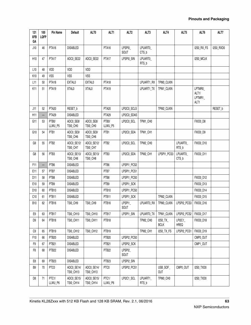
121XFBGA
100LQFP
Pin Name Default ALT0 ALT1 ALT2 ALT3 ALT4 ALT5 ALT6 ALT7
J10 46 PTA16 DISABLED PTA16 LPSPI0_SOUT
LPUART0_CTS_b
I2S0_RX_FS I2S0_RXD0
H10 47 PTA17 ADC0_SE22 ADC0_SE22 PTA17 LPSPI0_SIN LPUART0_RTS_b
I2S0_MCLK
L10 48 VDD VDD VDD
K10 49 VSS VSS VSS
L11 50 PTA18 EXTAL0 EXTAL0 PTA18 LPUART1_RX TPM0_CLKIN
K11 51 PTA19 XTAL0 XTAL0 PTA19 LPUART1_TX TPM1_CLKIN LPTMR0_ALT1/LPTMR1_ALT1
J11 52 PTA20 RESET_b PTA20 LPI2C0_SCLS TPM2_CLKIN RESET_b
H11 — PTA29 DISABLED PTA29 LPI2C0_SDAS
G11 53 PTB0/LLWU_P5
ADC0_SE8/TSI0_CH0
ADC0_SE8/TSI0_CH0
PTB0/LLWU_P5
LPI2C0_SCL TPM1_CH0 FXIO0_D8
G10 54 PTB1 ADC0_SE9/TSI0_CH6
ADC0_SE9/TSI0_CH6
PTB1 LPI2C0_SDA TPM1_CH1 FXIO0_D9
G9 55 PTB2 ADC0_SE12/TSI0_CH7
ADC0_SE12/TSI0_CH7
PTB2 LPI2C0_SCL TPM2_CH0 LPUART0_RTS_b
FXIO0_D10
G8 56 PTB3 ADC0_SE13/TSI0_CH8
ADC0_SE13/TSI0_CH8
PTB3 LPI2C0_SDA TPM2_CH1 LPSPI1_PCS3 LPUART0_CTS_b
FXIO0_D11
F11 — PTB6 DISABLED PTB6 LPSPI1_PCS2
E11 57 PTB7 DISABLED PTB7 LPSPI1_PCS1
D11 58 PTB8 DISABLED PTB8 LPSPI1_PCS0 FXIO0_D12
E10 59 PTB9 DISABLED PTB9 LPSPI1_SCK FXIO0_D13
D10 60 PTB10 DISABLED PTB10 LPSPI1_PCS0 FXIO0_D14
C10 61 PTB11 DISABLED PTB11 LPSPI1_SCK TPM2_CLKIN FXIO0_D15
B10 62 PTB16 TSI0_CH9 TSI0_CH9 PTB16 LPSPI1_SOUT
LPUART0_RX TPM0_CLKIN LPSPI2_PCS3 FXIO0_D16
E9 63 PTB17 TSI0_CH10 TSI0_CH10 PTB17 LPSPI1_SIN LPUART0_TX TPM1_CLKIN LPSPI2_PCS2 FXIO0_D17
D9 64 PTB18 TSI0_CH11 TSI0_CH11 PTB18 TPM2_CH0 I2S0_TX_BCLK
LPI2C1_HREQ
FXIO0_D18
C9 65 PTB19 TSI0_CH12 TSI0_CH12 PTB19 TPM2_CH1 I2S0_TX_FS LPSPI2_PCS1 FXIO0_D19
F10 66 PTB20 DISABLED PTB20 LPSPI2_PCS0 CMP0_OUT
F9 67 PTB21 DISABLED PTB21 LPSPI2_SCK CMP1_OUT
F8 68 PTB22 DISABLED PTB22 LPSPI2_SOUT
E8 69 PTB23 DISABLED PTB23 LPSPI2_SIN
B9 70 PTC0 ADC0_SE14/TSI0_CH13
ADC0_SE14/TSI0_CH13
PTC0 LPSPI2_PCS1 USB_SOF_OUT
CMP0_OUT I2S0_TXD0
D8 71 PTC1/LLWU_P6
ADC0_SE15/TSI0_CH14
ADC0_SE15/TSI0_CH14
PTC1/LLWU_P6
LPI2C1_SCL LPUART1_RTS_b
TPM0_CH0 I2S0_TXD0
Pinouts and Packaging
Kinetis KL28Zxxx with 512 KB Flash and 128 KB SRAM, Rev. 2.1, 06/2016 63
NXP Semiconductors
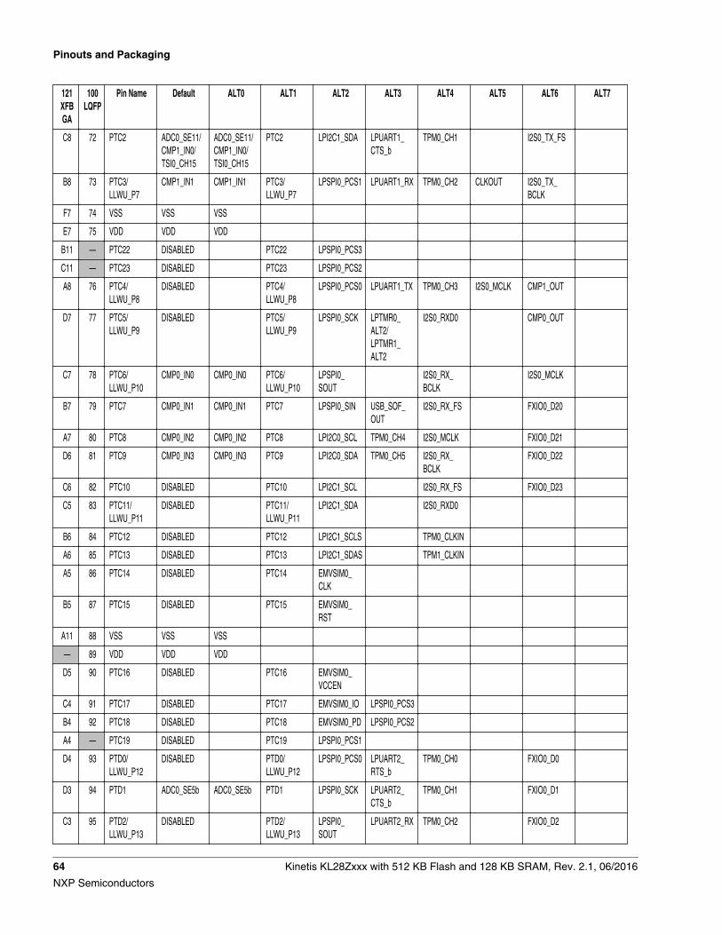
121XFBGA
100LQFP
Pin Name Default ALT0 ALT1 ALT2 ALT3 ALT4 ALT5 ALT6 ALT7
C8 72 PTC2 ADC0_SE11/CMP1_IN0/TSI0_CH15
ADC0_SE11/CMP1_IN0/TSI0_CH15
PTC2 LPI2C1_SDA LPUART1_CTS_b
TPM0_CH1 I2S0_TX_FS
B8 73 PTC3/LLWU_P7
CMP1_IN1 CMP1_IN1 PTC3/LLWU_P7
LPSPI0_PCS1 LPUART1_RX TPM0_CH2 CLKOUT I2S0_TX_BCLK
F7 74 VSS VSS VSS
E7 75 VDD VDD VDD
B11 — PTC22 DISABLED PTC22 LPSPI0_PCS3
C11 — PTC23 DISABLED PTC23 LPSPI0_PCS2
A8 76 PTC4/LLWU_P8
DISABLED PTC4/LLWU_P8
LPSPI0_PCS0 LPUART1_TX TPM0_CH3 I2S0_MCLK CMP1_OUT
D7 77 PTC5/LLWU_P9
DISABLED PTC5/LLWU_P9
LPSPI0_SCK LPTMR0_ALT2/LPTMR1_ALT2
I2S0_RXD0 CMP0_OUT
C7 78 PTC6/LLWU_P10
CMP0_IN0 CMP0_IN0 PTC6/LLWU_P10
LPSPI0_SOUT
I2S0_RX_BCLK
I2S0_MCLK
B7 79 PTC7 CMP0_IN1 CMP0_IN1 PTC7 LPSPI0_SIN USB_SOF_OUT
I2S0_RX_FS FXIO0_D20
A7 80 PTC8 CMP0_IN2 CMP0_IN2 PTC8 LPI2C0_SCL TPM0_CH4 I2S0_MCLK FXIO0_D21
D6 81 PTC9 CMP0_IN3 CMP0_IN3 PTC9 LPI2C0_SDA TPM0_CH5 I2S0_RX_BCLK
FXIO0_D22
C6 82 PTC10 DISABLED PTC10 LPI2C1_SCL I2S0_RX_FS FXIO0_D23
C5 83 PTC11/LLWU_P11
DISABLED PTC11/LLWU_P11
LPI2C1_SDA I2S0_RXD0
B6 84 PTC12 DISABLED PTC12 LPI2C1_SCLS TPM0_CLKIN
A6 85 PTC13 DISABLED PTC13 LPI2C1_SDAS TPM1_CLKIN
A5 86 PTC14 DISABLED PTC14 EMVSIM0_CLK
B5 87 PTC15 DISABLED PTC15 EMVSIM0_RST
A11 88 VSS VSS VSS
— 89 VDD VDD VDD
D5 90 PTC16 DISABLED PTC16 EMVSIM0_VCCEN
C4 91 PTC17 DISABLED PTC17 EMVSIM0_IO LPSPI0_PCS3
B4 92 PTC18 DISABLED PTC18 EMVSIM0_PD LPSPI0_PCS2
A4 — PTC19 DISABLED PTC19 LPSPI0_PCS1
D4 93 PTD0/LLWU_P12
DISABLED PTD0/LLWU_P12
LPSPI0_PCS0 LPUART2_RTS_b
TPM0_CH0 FXIO0_D0
D3 94 PTD1 ADC0_SE5b ADC0_SE5b PTD1 LPSPI0_SCK LPUART2_CTS_b
TPM0_CH1 FXIO0_D1
C3 95 PTD2/LLWU_P13
DISABLED PTD2/LLWU_P13
LPSPI0_SOUT
LPUART2_RX TPM0_CH2 FXIO0_D2
Pinouts and Packaging
64 Kinetis KL28Zxxx with 512 KB Flash and 128 KB SRAM, Rev. 2.1, 06/2016
NXP Semiconductors
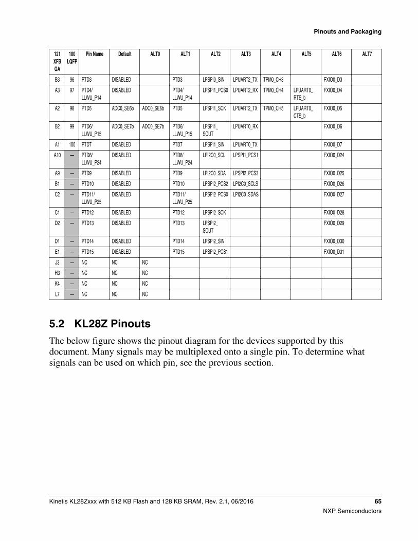
121XFBGA
100LQFP
Pin Name Default ALT0 ALT1 ALT2 ALT3 ALT4 ALT5 ALT6 ALT7
B3 96 PTD3 DISABLED PTD3 LPSPI0_SIN LPUART2_TX TPM0_CH3 FXIO0_D3
A3 97 PTD4/LLWU_P14
DISABLED PTD4/LLWU_P14
LPSPI1_PCS0 LPUART2_RX TPM0_CH4 LPUART0_RTS_b
FXIO0_D4
A2 98 PTD5 ADC0_SE6b ADC0_SE6b PTD5 LPSPI1_SCK LPUART2_TX TPM0_CH5 LPUART0_CTS_b
FXIO0_D5
B2 99 PTD6/LLWU_P15
ADC0_SE7b ADC0_SE7b PTD6/LLWU_P15
LPSPI1_SOUT
LPUART0_RX FXIO0_D6
A1 100 PTD7 DISABLED PTD7 LPSPI1_SIN LPUART0_TX FXIO0_D7
A10 — PTD8/LLWU_P24
DISABLED PTD8/LLWU_P24
LPI2C0_SCL LPSPI1_PCS1 FXIO0_D24
A9 — PTD9 DISABLED PTD9 LPI2C0_SDA LPSPI2_PCS3 FXIO0_D25
B1 — PTD10 DISABLED PTD10 LPSPI2_PCS2 LPI2C0_SCLS FXIO0_D26
C2 — PTD11/LLWU_P25
DISABLED PTD11/LLWU_P25
LPSPI2_PCS0 LPI2C0_SDAS FXIO0_D27
C1 — PTD12 DISABLED PTD12 LPSPI2_SCK FXIO0_D28
D2 — PTD13 DISABLED PTD13 LPSPI2_SOUT
FXIO0_D29
D1 — PTD14 DISABLED PTD14 LPSPI2_SIN FXIO0_D30
E1 — PTD15 DISABLED PTD15 LPSPI2_PCS1 FXIO0_D31
J3 — NC NC NC
H3 — NC NC NC
K4 — NC NC NC
L7 — NC NC NC
5.2 KL28Z Pinouts
The below figure shows the pinout diagram for the devices supported by thisdocument. Many signals may be multiplexed onto a single pin. To determine whatsignals can be used on which pin, see the previous section.
Pinouts and Packaging
Kinetis KL28Zxxx with 512 KB Flash and 128 KB SRAM, Rev. 2.1, 06/2016 65
NXP Semiconductors
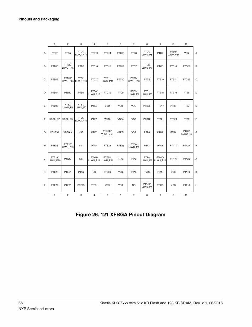
1
A PTD7
B PTD10
C PTD12
D PTD14
E PTD15
F USB0_DP
G VOUT33
H PTE16
J PTE18/LLWU_P20
K PTE20
1
L PTE22
2
PTD5
PTD6/LLWU_P15
PTD11/LLWU_P25
PTD13
PTE2/LLWU_P1
USB0_DM
VREGIN
PTE17/LLWU_P19
PTE19
PTE21
2
PTE23
3
PTD4/LLWU_P14
PTD3
PTD2/LLWU_P13
PTD1
PTE1/LLWU_P0
PTE6/LLWU_P16
VSS
NC
NC
PTA6
3
PTE29
4
PTC19
PTC18
PTC17
PTD0/LLWU_P12
PTE0
PTE3
PTE5
PTA7
PTA11/LLWU_P23
NC
4
PTE31
5
PTC14
PTC15
PTC11/LLWU_P11
PTC16
VDD
VDDA
VREFH/VREF_OUT
PTE24
PTE25/LLWU_P21
PTE30
5
VSS
6
PTC13
PTC12
PTC10
PTC9
VDD
VSSA
VREFL
PTE26
PTA0
VDD
6
VSS
7
PTC8
PTC7
PTC6/LLWU_P10
PTC5/LLWU_P9
VDD
VSS
VSS
PTE4/LLWU_P2
PTA2
PTA5
7
NC
8
PTC4/LLWU_P8
PTC3/LLWU_P7
PTC2
PTC1/LLWU_P6
PTB23
PTB22
PTB3
PTA1
PTA4/LLWU_P3
PTA12
8
PTA13/LLWU_P4
9
PTD9
PTC0
PTB19
PTB18
PTB17
PTB21
PTB2
PTA3
PTA10/LLWU_P22
PTA14
9
PTA15
10
PTD8/LLWU_P24
PTB16
PTB11
PTB10
PTB9
PTB20
PTB1
PTA17
PTA16
VSS
10
VDD
11
AVSS
BPTC22
CPTC23
DPTB8
EPTB7
FPTB6
GPTB0/LLWU_P5
HPTA29
JPTA20
KPTA19
11
LPTA18
Figure 26. 121 XFBGA Pinout Diagram
Pinouts and Packaging
66 Kinetis KL28Zxxx with 512 KB Flash and 128 KB SRAM, Rev. 2.1, 06/2016
NXP Semiconductors

60
59
58
57
56
55
54
53
52
51
20
19
18
17
16
15
14
13
12
11
10
9
8
7
6
5
4
3
2
1
PTE22
PTE21
PTE20
PTE19
PTE18/LLWU_P20
PTE17/LLWU_P19
PTE16
VREGIN
VOUT33
USB0_DM
USB0_DP
VSS
VDD
PTE6/LLWU_P16
PTE5
PTE4/LLWU_P2
PTE3
PTE2/LLWU_P1
PTE1/LLWU_P0
PTE0 75
74
73
72
71
70
69
68
67
66
65
64
63
62
61
VDD
VSS
PTC3/LLWU_P7
PTC2
PTC1/LLWU_P6
PTC0
PTB23
PTB22
PTB21
PTB20
PTB19
PTB18
PTB17
PTB16
PTB11
PTB10
PTB9
PTB8
PTB7
PTB3
PTB2
PTB1
PTB0/LLWU_P5
PTA20
PTA1925
24
23
22
21
VSSA
VREFL
VREFH/VREF_OUT
VDDA
PTE23
403938373635343332313029282726
99 79 78 77 76
PT
D6/
LLW
U_P
15
PT
C7
PT
C6/
LLW
U_P
10
PT
C5/
LLW
U_P
9
PT
C4/
LLW
U_P
850494847464544434241
PTA
18
VS
S
VD
D
PTA
17
PTA
16
PTA
15
PTA
14
PTA
13/L
LWU
_P4
PTA
12
PTA
7
PTA
6
PTA
5
PTA
4/LL
WU
_P3
PTA
3
PTA
2
PTA
1
PTA
0
PT
E26
PT
E25
/LLW
U_P
21
PT
E24
VD
D
VS
S
PT
E31
PT
E30
PT
E29
98P
TD
5
97P
TD
4/LL
WU
_P14
96P
TD
3
95P
TD
2/LL
WU
_P13
94P
TD
1
93P
TD
0/LL
WU
_P12
92P
TC
18
91P
TC
17
90P
TC
16
89V
DD
88V
SS
80P
TC
8
PT
C9
PT
C10
818283P
TC
11/L
LWU
_P11
84P
TC
12
85P
TC
13
86P
TC
14
87P
TC
15
100
PT
D7
Figure 27. 100 LQFP Pinout Diagram
6 Ordering parts
Ordering parts
Kinetis KL28Zxxx with 512 KB Flash and 128 KB SRAM, Rev. 2.1, 06/2016 67
NXP Semiconductors
6.1 Determining valid orderable parts
Valid orderable part numbers are provided on the web. To determine the orderable partnumbers for this device, go to nxp.com and perform a part number search for thefollowing device numbers: PKL28Z and MKL28Z
7 Design considerations
7.1 Hardware design considerations
This device contains protective circuitry to guard against damage due to high staticvoltage or electric fields. However, take normal precautions to avoid application of anyvoltages higher than maximum-rated voltages to this high-impedance circuit.
7.1.1 Printed circuit board recommendations• Place connectors or cables on one edge of the board and do not place digital circuits
between connectors.• Drivers and filters for I/O functions must be placed as close to the connectors as
possible. Connect TVS devices at the connector to a good ground. Connect filtercapacitors at the connector to a good ground.
• Physically isolate analog circuits from digital circuits if possible.• Place input filter capacitors as close to the MCU as possible.• For best EMC performance, route signals as transmission lines; use a ground plane
directly under LQFP/MAPBGA packages.
7.1.2 Power delivery systemConsider the following items in the power delivery system:
• Use a plane for ground.• Use a plane for MCU VDD supply if possible.• Always route ground first, as a plane or continuous surface, and never as sequential
segments.• Route power next, as a plane or traces that are parallel to ground traces.• Place bulk capacitance, 10 μF or more, at the entrance of the power plane.• Place bypass capacitors for MCU power domain as close as possible to each
VDD/VSS pair, including VDDA/VSSA and VREFH/VREFL.
Design considerations
68 Kinetis KL28Zxxx with 512 KB Flash and 128 KB SRAM, Rev. 2.1, 06/2016
NXP Semiconductors
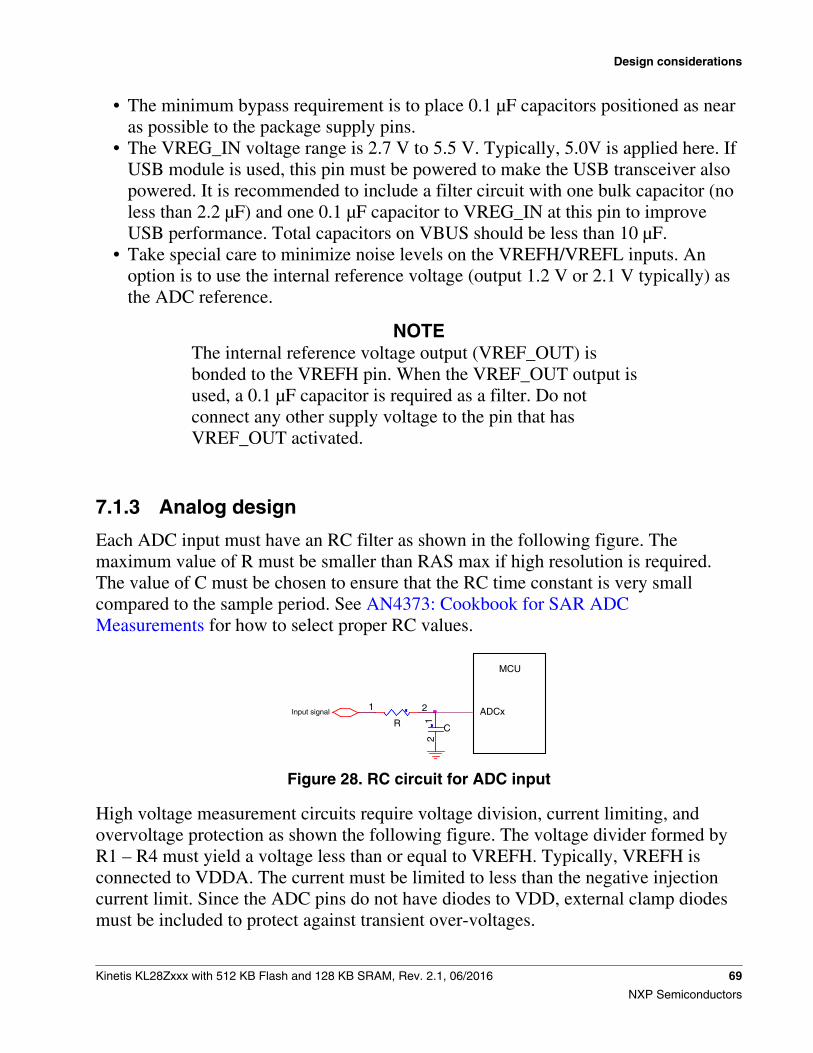
• The minimum bypass requirement is to place 0.1 μF capacitors positioned as nearas possible to the package supply pins.
• The VREG_IN voltage range is 2.7 V to 5.5 V. Typically, 5.0V is applied here. IfUSB module is used, this pin must be powered to make the USB transceiver alsopowered. It is recommended to include a filter circuit with one bulk capacitor (noless than 2.2 μF) and one 0.1 μF capacitor to VREG_IN at this pin to improveUSB performance. Total capacitors on VBUS should be less than 10 μF.
• Take special care to minimize noise levels on the VREFH/VREFL inputs. Anoption is to use the internal reference voltage (output 1.2 V or 2.1 V typically) asthe ADC reference.
NOTEThe internal reference voltage output (VREF_OUT) isbonded to the VREFH pin. When the VREF_OUT output isused, a 0.1 μF capacitor is required as a filter. Do notconnect any other supply voltage to the pin that hasVREF_OUT activated.
7.1.3 Analog design
Each ADC input must have an RC filter as shown in the following figure. Themaximum value of R must be smaller than RAS max if high resolution is required.The value of C must be chosen to ensure that the RC time constant is very smallcompared to the sample period. See AN4373: Cookbook for SAR ADCMeasurements for how to select proper RC values.
MCU
ADCx
CRInput signal
1 2
12
Figure 28. RC circuit for ADC input
High voltage measurement circuits require voltage division, current limiting, andovervoltage protection as shown the following figure. The voltage divider formed byR1 – R4 must yield a voltage less than or equal to VREFH. Typically, VREFH isconnected to VDDA. The current must be limited to less than the negative injectioncurrent limit. Since the ADC pins do not have diodes to VDD, external clamp diodesmust be included to protect against transient over-voltages.
Design considerations
Kinetis KL28Zxxx with 512 KB Flash and 128 KB SRAM, Rev. 2.1, 06/2016 69
NXP Semiconductors
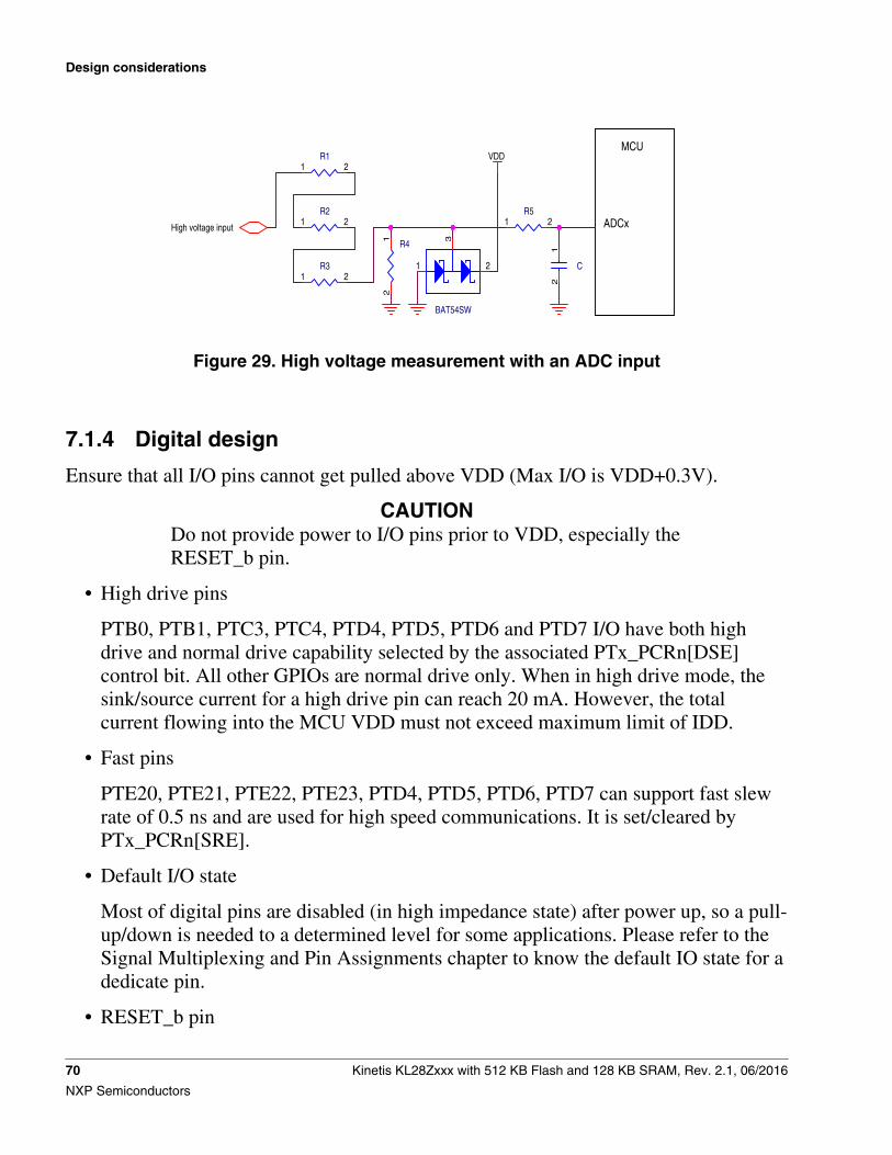
5
5
4
4
3
3
2
2
1
1
D D
C C
B B
A A
EXTAL XTAL
OSCILLATOR
EXTAL XTAL
OSCILLATOR
EXTAL XTAL
OSCILLATOR
EXTAL XTAL
OSCILLATOR
EXTAL XTAL
OSCILLATOR
EXTAL XTAL
OSCILLATOR
MCU
ADCx
MCU
ADCx
MCU
RESET_b
MCU
NMI_b
MCU
RESET_b
Supervisor Chip
OUT
Active high,open drain
RESET_b
SWD_DIOSWD_CLK
Analog input
High voltage input
RESET_b
VDD
VDD
VDD
VDD
VDD
VDD
Drawing Title:
Size Document Number Rev
Date: Sheet of
Page Title:
ICAP Classification: FCP: FIUO: PUBI:
SCH-XXXXX PDF: SPF-XXXXX X
<Title>
C
Friday, February 06, 2015
<PageTitle>
1 1
___ ___XDrawing Title:
Size Document Number Rev
Date: Sheet of
Page Title:
ICAP Classification: FCP: FIUO: PUBI:
SCH-XXXXX PDF: SPF-XXXXX X
<Title>
C
Friday, February 06, 2015
<PageTitle>
1 1
___ ___XDrawing Title:
Size Document Number Rev
Date: Sheet of
Page Title:
ICAP Classification: FCP: FIUO: PUBI:
SCH-XXXXX PDF: SPF-XXXXX X
<Title>
C
Friday, February 06, 2015
<PageTitle>
1 1
___ ___X
R
1 2
0.1uF
12
R51 2
Cx
12
0.1uF
12
RESONATOR
1 3
2Cy
12
Cx
12
CRYSTAL
21
J1
HDR_5X2
1 23 4
657 89 10
Cy
12
10k
12
10k
12
R412
CRYSTAL
21
0.1uF
12
10k
12
CRYSTAL
21
R11 2
R31 2
C
12
RESONATOR
1 3
2
R21 2
10k
12
10k
12
RF
1 2
RS
12
BAT54SW
1 2
3
RS
12
RS
12
C
12
RF
1 2
RS
1 2
RF
1 2
CRYSTAL
21
Figure 29. High voltage measurement with an ADC input
7.1.4 Digital design
Ensure that all I/O pins cannot get pulled above VDD (Max I/O is VDD+0.3V).
CAUTIONDo not provide power to I/O pins prior to VDD, especially theRESET_b pin.
• High drive pins
PTB0, PTB1, PTC3, PTC4, PTD4, PTD5, PTD6 and PTD7 I/O have both highdrive and normal drive capability selected by the associated PTx_PCRn[DSE]control bit. All other GPIOs are normal drive only. When in high drive mode, thesink/source current for a high drive pin can reach 20 mA. However, the totalcurrent flowing into the MCU VDD must not exceed maximum limit of IDD.
• Fast pins
PTE20, PTE21, PTE22, PTE23, PTD4, PTD5, PTD6, PTD7 can support fast slewrate of 0.5 ns and are used for high speed communications. It is set/cleared byPTx_PCRn[SRE].
• Default I/O state
Most of digital pins are disabled (in high impedance state) after power up, so a pull-up/down is needed to a determined level for some applications. Please refer to theSignal Multiplexing and Pin Assignments chapter to know the default IO state for adedicate pin.
• RESET_b pin
Design considerations
70 Kinetis KL28Zxxx with 512 KB Flash and 128 KB SRAM, Rev. 2.1, 06/2016
NXP Semiconductors
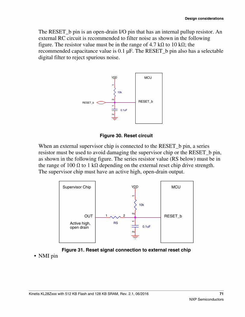
The RESET_b pin is an open-drain I/O pin that has an internal pullup resistor. Anexternal RC circuit is recommended to filter noise as shown in the followingfigure. The resistor value must be in the range of 4.7 kΩ to 10 kΩ; therecommended capacitance value is 0.1 μF. The RESET_b pin also has a selectabledigital filter to reject spurious noise.
5
5
4
4
3
3
2
2
1
1
D D
C C
B B
A A
EXTAL XTAL OSCILLATOR
EXTAL XTAL OSCILLATOR
EXTAL XTAL OSCILLATOR EXTAL XTAL OSCILLATOR
EXTAL XTAL OSCILLATOR EXTAL XTAL OSCILLATOR
MCU
ADCx
MCU
ADCx
MCU
RESET_b
MCU
NMI_b
MCU
RESET_b
Supervisor Chip
OUT Active high, open drain
RESET_b
SWD_DIOSWD_CLK
Analog input
High voltage input
RESET_b
VDD
VDD
VDD
VDD
VDD
VDD
Drawing Title: Size Document Number Rev Date: Sheet of Page Title:
ICAP Classification: FCP: FIUO: PUBI:
SCH-XXXXX PDF: SPF-XXXXX X
<Title>
C Friday, February 06, 2015
<PageTitle>
1 1
___ ___ X Drawing Title: Size Document Number Rev Date: Sheet of Page Title:
ICAP Classification: FCP: FIUO: PUBI:
SCH-XXXXX PDF: SPF-XXXXX X
<Title>
C Friday, February 06, 2015
<PageTitle>
1 1
___ ___ X Drawing Title: Size Document Number Rev Date: Sheet of Page Title:
ICAP Classification: FCP: FIUO: PUBI:
SCH-XXXXX PDF: SPF-XXXXX X
<Title>
C Friday, February 06, 2015
<PageTitle>
1 1
___ ___ X
R
1 2
0.1uF1
2
R51 2
Cx
12
0.1uF
12
RESONATOR
1 3
2Cy
12
Cx
12
CRYSTAL
21
J1
HDR_5X2
1 23 4
657 89 10
Cy
12
10k
12
10k
12
R412
CRYSTAL
21
0.1uF
12
10k
12
CRYSTAL
21
R11 2
R31 2
C
12
RESONATOR
1 3
2
R21 2
10k
12
10k
12
RF
1 2
RS
12
BAT54SW
1 2
3
RS
12
RS
12
C
12
RF
1 2
RS
1 2
RF
1 2
CRYSTAL
21
Figure 30. Reset circuit
When an external supervisor chip is connected to the RESET_b pin, a seriesresistor must be used to avoid damaging the supervisor chip or the RESET_b pin,as shown in the following figure. The series resistor value (RS below) must be inthe range of 100 Ω to 1 kΩ depending on the external reset chip drive strength.The supervisor chip must have an active high, open-drain output.
5
5
4
4
3
3
2
2
1
1
D D
C C
B B
A A
EXTAL XTAL OSCILLATOR
EXTAL XTAL OSCILLATOR
EXTAL XTAL OSCILLATOR EXTAL XTAL OSCILLATOR
EXTAL XTAL OSCILLATOR EXTAL XTAL OSCILLATOR
MCU
ADCx
MCU
ADCx
MCU
RESET_b
MCU
NMI_b
MCU
RESET_b
Supervisor Chip
OUT Active high, open drain
RESET_b
SWD_DIOSWD_CLK
Analog input
High voltage input
RESET_b
VDD
VDD
VDD
VDD
VDD
VDD
Drawing Title: Size Document Number Rev Date: Sheet of Page Title:
ICAP Classification: FCP: FIUO: PUBI:
SCH-XXXXX PDF: SPF-XXXXX X
<Title>
C Friday, February 06, 2015
<PageTitle>
1 1
___ ___ X Drawing Title: Size Document Number Rev Date: Sheet of Page Title:
ICAP Classification: FCP: FIUO: PUBI:
SCH-XXXXX PDF: SPF-XXXXX X
<Title>
C Friday, February 06, 2015
<PageTitle>
1 1
___ ___ X Drawing Title: Size Document Number Rev Date: Sheet of Page Title:
ICAP Classification: FCP: FIUO: PUBI:
SCH-XXXXX PDF: SPF-XXXXX X
<Title>
C Friday, February 06, 2015
<PageTitle>
1 1
___ ___ X
R
1 2
0.1uF
12
R51 2
Cx
12
0.1uF
12
RESONATOR
1 3
2Cy
12
Cx
12
CRYSTAL
21
J1
HDR_5X2
1 23 4
657 89 10
Cy
12
10k
12
10k
12
R412
CRYSTAL
21
0.1uF
12
10k
12
CRYSTAL
21
R11 2
R31 2
C
12
RESONATOR
1 3
2
R21 2
10k
12
10k
12
RF
1 2
RS
12
BAT54SW
1 23
RS
12
RS
12
C
12
RF
1 2
RS
1 2
RF
1 2
CRYSTAL
21
Figure 31. Reset signal connection to external reset chip• NMI pin
Design considerations
Kinetis KL28Zxxx with 512 KB Flash and 128 KB SRAM, Rev. 2.1, 06/2016 71
NXP Semiconductors
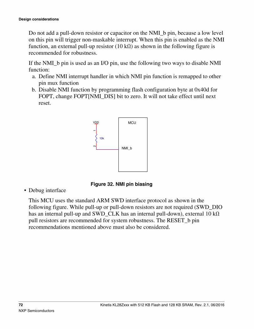
Do not add a pull-down resistor or capacitor on the NMI_b pin, because a low levelon this pin will trigger non-maskable interrupt. When this pin is enabled as the NMIfunction, an external pull-up resistor (10 kΩ) as shown in the following figure isrecommended for robustness.
If the NMI_b pin is used as an I/O pin, use the following two ways to disable NMIfunction:
a. Define NMI interrupt handler in which NMI pin function is remapped to otherpin mux function
b. Disable NMI function by programming flash configuration byte at 0x40d forFOPT, change FOPT[NMI_DIS] bit to zero. It will not take effect until nextreset.
5
5
4
4
3
3
2
2
1
1
D D
C C
B B
A A
EXTAL XTAL OSCILLATOR
EXTAL XTAL OSCILLATOR
EXTAL XTAL OSCILLATOR EXTAL XTAL OSCILLATOR
EXTAL XTAL OSCILLATOR EXTAL XTAL OSCILLATOR
MCU
ADCx
MCU
ADCx
MCU
RESET_b
MCU
NMI_b
MCU
RESET_b
Supervisor Chip
OUT Active high, open drain
RESET_b
SWD_DIOSWD_CLK
Analog input
High voltage input
RESET_b
VDD
VDD
VDD
VDD
VDD
VDD
Drawing Title: Size Document Number Rev Date: Sheet of Page Title:
ICAP Classification: FCP: FIUO: PUBI:
SCH-XXXXX PDF: SPF-XXXXX X
<Title>
C Friday, February 06, 2015
<PageTitle>
1 1
___ ___ X Drawing Title: Size Document Number Rev Date: Sheet of Page Title:
ICAP Classification: FCP: FIUO: PUBI:
SCH-XXXXX PDF: SPF-XXXXX X
<Title>
C Friday, February 06, 2015
<PageTitle>
1 1
___ ___ X Drawing Title: Size Document Number Rev Date: Sheet of Page Title:
ICAP Classification: FCP: FIUO: PUBI:
SCH-XXXXX PDF: SPF-XXXXX X
<Title>
C Friday, February 06, 2015
<PageTitle>
1 1
___ ___ X
R
1 2
0.1uF
12
R51 2
Cx
12
0.1uF
12
RESONATOR
1 3
2Cy
12
Cx
12
CRYSTAL
21
J1
HDR_5X2
1 23 4
657 89 10
Cy
12
10k
12
10k
12
R412
CRYSTAL
21
0.1uF
12
10k
12
CRYSTAL
21
R11 2
R31 2
C
12
RESONATOR
1 3
2
R21 2
10k
12
10k
12
RF
1 2
RS
12
BAT54SW
1 2
3
RS
12
RS
12
C
12
RF
1 2
RS
1 2
RF
1 2
CRYSTAL
21
Figure 32. NMI pin biasing• Debug interface
This MCU uses the standard ARM SWD interface protocol as shown in thefollowing figure. While pull-up or pull-down resistors are not required (SWD_DIOhas an internal pull-up and SWD_CLK has an internal pull-down), external 10 kΩpull resistors are recommended for system robustness. The RESET_b pinrecommendations mentioned above must also be considered.
Design considerations
72 Kinetis KL28Zxxx with 512 KB Flash and 128 KB SRAM, Rev. 2.1, 06/2016
NXP Semiconductors
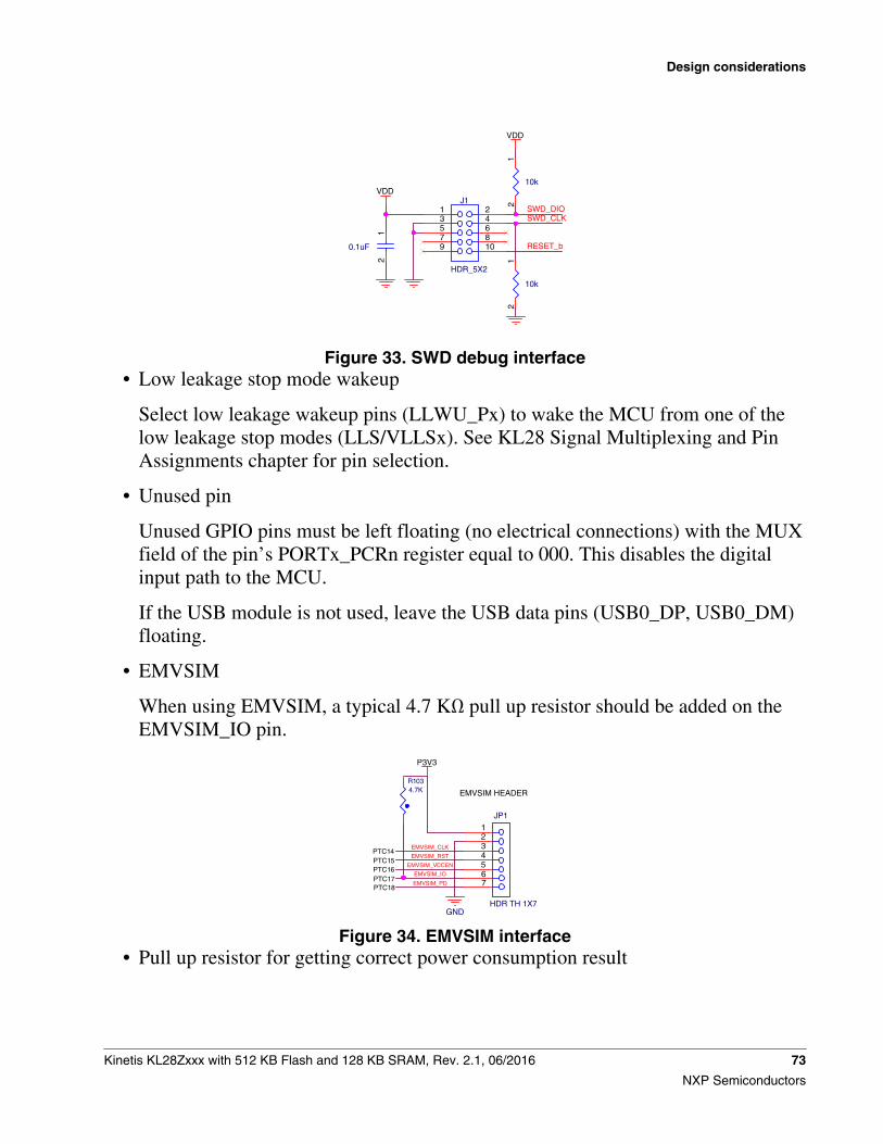
5
5
4
4
3
3
2
2
1
1
D D
C C
B B
A A
EXTAL XTAL OSCILLATOR
EXTAL XTAL OSCILLATOR
EXTAL XTAL OSCILLATOR EXTAL XTAL OSCILLATOR
EXTAL XTAL OSCILLATOR EXTAL XTAL OSCILLATOR
MCU
ADCx
MCU
ADCx
MCU
RESET_b
MCU
NMI_b
MCU
RESET_b
Supervisor Chip
OUT Active high, open drain
RESET_b
SWD_DIOSWD_CLK
Analog input
High voltage input
RESET_b
VDD
VDD
VDD
VDD
VDD
VDD
Drawing Title: Size Document Number Rev Date: Sheet of Page Title:
ICAP Classification: FCP: FIUO: PUBI:
SCH-XXXXX PDF: SPF-XXXXX X
<Title>
C Friday, February 06, 2015
<PageTitle>
1 1
___ ___ X Drawing Title: Size Document Number Rev Date: Sheet of Page Title:
ICAP Classification: FCP: FIUO: PUBI:
SCH-XXXXX PDF: SPF-XXXXX X
<Title>
C Friday, February 06, 2015
<PageTitle>
1 1
___ ___ X Drawing Title: Size Document Number Rev Date: Sheet of Page Title:
ICAP Classification: FCP: FIUO: PUBI:
SCH-XXXXX PDF: SPF-XXXXX X
<Title>
C Friday, February 06, 2015
<PageTitle>
1 1
___ ___ X
R
1 2
0.1uF
12
R51 2
Cx
12
0.1uF
12
RESONATOR
1 3
2Cy
12
Cx
12
CRYSTAL
21
J1
HDR_5X2
1 23 4
657 89 10
Cy
12
10k
12
10k
12
R412
CRYSTAL
21
0.1uF
12
10k
12
CRYSTAL
21
R11 2
R31 2
C
12
RESONATOR
1 3
2
R21 2
10k
12
10k
12
RF
1 2
RS
12
BAT54SW
1 2
3
RS
12
RS
12
C
12
RF
1 2
RS
1 2
RF
1 2
CRYSTAL
21
Figure 33. SWD debug interface• Low leakage stop mode wakeup
Select low leakage wakeup pins (LLWU_Px) to wake the MCU from one of thelow leakage stop modes (LLS/VLLSx). See KL28 Signal Multiplexing and PinAssignments chapter for pin selection.
• Unused pin
Unused GPIO pins must be left floating (no electrical connections) with the MUXfield of the pin’s PORTx_PCRn register equal to 000. This disables the digitalinput path to the MCU.
If the USB module is not used, leave the USB data pins (USB0_DP, USB0_DM)floating.
• EMVSIM
When using EMVSIM, a typical 4.7 KΩ pull up resistor should be added on theEMVSIM_IO pin.
5
5
4
4
3
3
2
2
1
1
D D
C C
B B
A A
EXTAL XTAL OSCILLATOR
EXTAL XTAL OSCILLATOR
EXTAL XTAL OSCILLATOR EXTAL XTAL OSCILLATOR
EXTAL XTAL OSCILLATOR EXTAL XTAL OSCILLATOR
MCU
ADCx
MCU
ADCx
MCU
RESET_b
MCU
NMI_b
MCU
RESET_b
Supervisor Chip
OUT Active high, open drain
Analog input
High voltage input
RESET_b
VDD
VDD
VDD
VDD
Drawing Title: Size Document Number Rev Date: Sheet of Page Title:
ICAP Classification: FCP: FIUO: PUBI:
SCH-XXXXX PDF: SPF-XXXXX X
<Title>
C Friday, February 06, 2015
<PageTitle>
1 1
___ ___ X Drawing Title: Size Document Number Rev Date: Sheet of Page Title:
ICAP Classification: FCP: FIUO: PUBI:
SCH-XXXXX PDF: SPF-XXXXX X
<Title>
C Friday, February 06, 2015
<PageTitle>
1 1
___ ___ X Drawing Title: Size Document Number Rev Date: Sheet of Page Title:
ICAP Classification: FCP: FIUO: PUBI:
SCH-XXXXX PDF: SPF-XXXXX X
<Title>
C Friday, February 06, 2015
<PageTitle>
1 1
___ ___ X
R
1 2
0.1uF
12
R51 2
Cx
12
RESONATOR
1 3
2Cy
12
Cx
12
CRYSTAL
21
Cy
12
10k
12
R412
CRYSTAL
21
0.1uF
12
CRYSTAL
21
R11 2
R31 2
C
12
RESONATOR
1 3
2
R21 2
10k
12
10k
12
RF
1 2
RS
12
BAT54SW
1 2
3
RS
12
RS
12
C1
2
RF
1 2
RS
1 2
RF
1 2
CRYSTAL
21
P3V3
12345
HDR TH 1X7
JP1
67
GND
PTC14PTC15PTC16PTC17PTC18
EMVSIM_CLK
R103 4.7K
EMVSIM_RST
EMVSIM_IO
EMVSIM_VCCEN
EMVSIM_PD
EMVSIM HEADER
Figure 34. EMVSIM interface• Pull up resistor for getting correct power consumption result
Design considerations
Kinetis KL28Zxxx with 512 KB Flash and 128 KB SRAM, Rev. 2.1, 06/2016 73
NXP Semiconductors
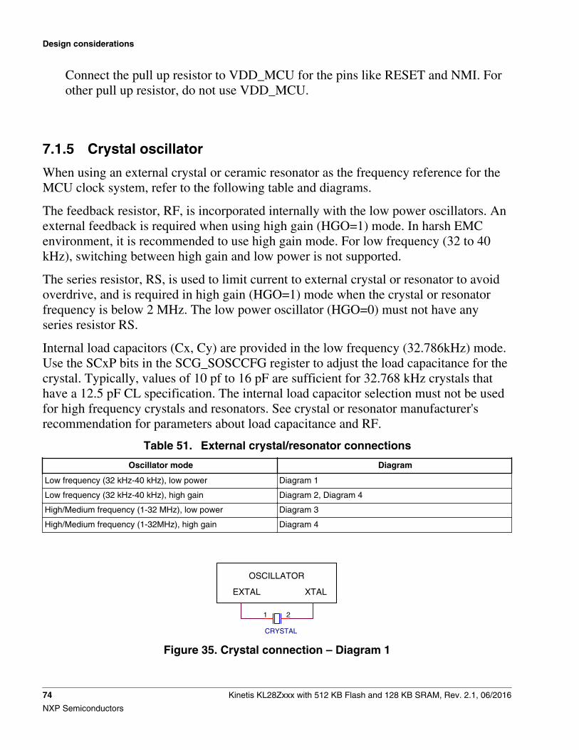
Connect the pull up resistor to VDD_MCU for the pins like RESET and NMI. Forother pull up resistor, do not use VDD_MCU.
7.1.5 Crystal oscillator
When using an external crystal or ceramic resonator as the frequency reference for theMCU clock system, refer to the following table and diagrams.
The feedback resistor, RF, is incorporated internally with the low power oscillators. Anexternal feedback is required when using high gain (HGO=1) mode. In harsh EMCenvironment, it is recommended to use high gain mode. For low frequency (32 to 40kHz), switching between high gain and low power is not supported.
The series resistor, RS, is used to limit current to external crystal or resonator to avoidoverdrive, and is required in high gain (HGO=1) mode when the crystal or resonatorfrequency is below 2 MHz. The low power oscillator (HGO=0) must not have anyseries resistor RS.
Internal load capacitors (Cx, Cy) are provided in the low frequency (32.786kHz) mode.Use the SCxP bits in the SCG_SOSCCFG register to adjust the load capacitance for thecrystal. Typically, values of 10 pf to 16 pF are sufficient for 32.768 kHz crystals thathave a 12.5 pF CL specification. The internal load capacitor selection must not be usedfor high frequency crystals and resonators. See crystal or resonator manufacturer'srecommendation for parameters about load capacitance and RF.
Table 51. External crystal/resonator connections
Oscillator mode Diagram
Low frequency (32 kHz-40 kHz), low power Diagram 1
Low frequency (32 kHz-40 kHz), high gain Diagram 2, Diagram 4
High/Medium frequency (1-32 MHz), low power Diagram 3
High/Medium frequency (1-32MHz), high gain Diagram 45
5
4
4
3
3
2
2
1
1
D D
C C
B B
A A
EXTAL XTAL OSCILLATOR
EXTAL XTAL OSCILLATOR
EXTAL XTAL OSCILLATOR EXTAL XTAL OSCILLATOR
EXTAL XTAL OSCILLATOR EXTAL XTAL OSCILLATOR
MCU
ADCx
MCU
ADCx
MCU
RESET_b
MCU
NMI_b
MCU
RESET_b
Supervisor Chip
OUT Active high, open drain
RESET_b
SWD_DIOSWD_CLK
Analog input
High voltage input
RESET_b
VDD
VDD
VDD
VDD
VDD
VDD
Drawing Title: Size Document Number Rev Date: Sheet of Page Title:
ICAP Classification: FCP: FIUO: PUBI:
SCH-XXXXX PDF: SPF-XXXXX X
<Title>
C Friday, February 06, 2015
<PageTitle>
1 1
___ ___ X Drawing Title: Size Document Number Rev Date: Sheet of Page Title:
ICAP Classification: FCP: FIUO: PUBI:
SCH-XXXXX PDF: SPF-XXXXX X
<Title>
C Friday, February 06, 2015
<PageTitle>
1 1
___ ___ X Drawing Title: Size Document Number Rev Date: Sheet of Page Title:
ICAP Classification: FCP: FIUO: PUBI:
SCH-XXXXX PDF: SPF-XXXXX X
<Title>
C Friday, February 06, 2015
<PageTitle>
1 1
___ ___ X
R
1 2
0.1uF
12
R51 2
Cx
12
0.1uF
12
RESONATOR
1 3
2Cy
12
Cx
12
CRYSTAL
21
J1
HDR_5X2
1 23 4
657 89 10
Cy
12
10k
12
10k
12
R412
CRYSTAL
21
0.1uF
12
10k
12
CRYSTAL
21
R11 2
R31 2
C
12
RESONATOR
1 3
2
R21 2
10k
12
10k
12
RF
1 2
RS
12
BAT54SW
1 2
3
RS
12
RS
12
C
12
RF
1 2
RS
1 2
RF
1 2
CRYSTAL
21
Figure 35. Crystal connection – Diagram 1
Design considerations
74 Kinetis KL28Zxxx with 512 KB Flash and 128 KB SRAM, Rev. 2.1, 06/2016
NXP Semiconductors
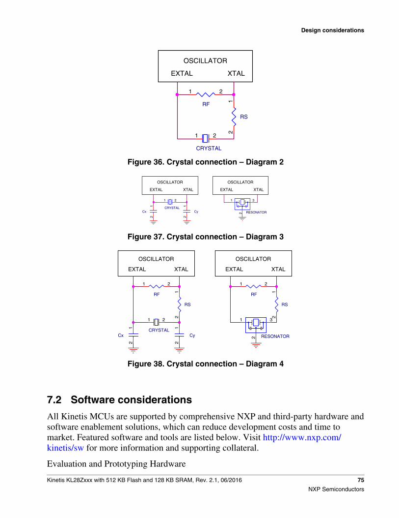
5
5
4
4
3
3
2
2
1
1
D D
C C
B B
A A
EXTAL XTAL OSCILLATOR
EXTAL XTAL OSCILLATOR
EXTAL XTAL OSCILLATOR EXTAL XTAL OSCILLATOR
EXTAL XTAL OSCILLATOR EXTAL XTAL OSCILLATOR
MCU
ADCx
MCU
ADCx
MCU
RESET_b
MCU
NMI_b
MCU
RESET_b
Supervisor Chip
OUT Active high, open drain
RESET_b
SWD_DIOSWD_CLK
Analog input
High voltage input
RESET_b
VDD
VDD
VDD
VDD
VDD
VDD
Drawing Title: Size Document Number Rev Date: Sheet of Page Title:
ICAP Classification: FCP: FIUO: PUBI:
SCH-XXXXX PDF: SPF-XXXXX X
<Title>
C Friday, February 06, 2015
<PageTitle>
1 1
___ ___ X Drawing Title: Size Document Number Rev Date: Sheet of Page Title:
ICAP Classification: FCP: FIUO: PUBI:
SCH-XXXXX PDF: SPF-XXXXX X
<Title>
C Friday, February 06, 2015
<PageTitle>
1 1
___ ___ X Drawing Title: Size Document Number Rev Date: Sheet of Page Title:
ICAP Classification: FCP: FIUO: PUBI:
SCH-XXXXX PDF: SPF-XXXXX X
<Title>
C Friday, February 06, 2015
<PageTitle>
1 1
___ ___ X
R
1 2
0.1uF
12
R51 2
Cx
12
0.1uF
12
RESONATOR
1 3
2Cy
12
Cx
12
CRYSTAL
21
J1
HDR_5X2
1 23 4
657 89 10
Cy
12
10k
12
10k
12
R412
CRYSTAL
21
0.1uF
12
10k
12
CRYSTAL
21
R11 2
R31 2
C
12
RESONATOR
1 3
2
R21 2
10k
12
10k
12
RF
1 2
RS
12
BAT54SW
1 2
3
RS
12
RS
12
C
12
RF
1 2
RS
1 2
RF
1 2
CRYSTAL
21
Figure 36. Crystal connection – Diagram 25
5
4
4
3
3
2
2
1
1
D D
C C
B B
A A
EXTAL XTAL OSCILLATOR
EXTAL XTAL OSCILLATOR
EXTAL XTAL OSCILLATOR EXTAL XTAL OSCILLATOR
EXTAL XTAL OSCILLATOR EXTAL XTAL OSCILLATOR
MCU
ADCx
MCU
ADCx
MCU
RESET_b
MCU
NMI_b
MCU
RESET_b
Supervisor Chip
OUT Active high, open drain
RESET_b
SWD_DIOSWD_CLK
Analog input
High voltage input
RESET_b
VDD
VDD
VDD
VDD
VDD
VDD
Drawing Title: Size Document Number Rev Date: Sheet of Page Title:
ICAP Classification: FCP: FIUO: PUBI:
SCH-XXXXX PDF: SPF-XXXXX X
<Title>
C Friday, February 06, 2015
<PageTitle>
1 1
___ ___ X Drawing Title: Size Document Number Rev Date: Sheet of Page Title:
ICAP Classification: FCP: FIUO: PUBI:
SCH-XXXXX PDF: SPF-XXXXX X
<Title>
C Friday, February 06, 2015
<PageTitle>
1 1
___ ___ X Drawing Title: Size Document Number Rev Date: Sheet of Page Title:
ICAP Classification: FCP: FIUO: PUBI:
SCH-XXXXX PDF: SPF-XXXXX X
<Title>
C Friday, February 06, 2015
<PageTitle>
1 1
___ ___ X
R
1 2
0.1uF
12
R51 2
Cx
12
0.1uF
12
RESONATOR
1 3
2Cy
12
Cx
12
CRYSTAL
21
J1
HDR_5X2
1 23 4
657 89 10
Cy
12
10k
12
10k
12
R412
CRYSTAL
21
0.1uF
12
10k
12
CRYSTAL
21
R11 2
R31 2
C
12
RESONATOR
1 3
2
R21 2
10k
12
10k
12
RF
1 2
RS
12
BAT54SW
1 2
3
RS
12
RS
12
C
12
RF
1 2
RS
1 2
RF
1 2
CRYSTAL
21
Figure 37. Crystal connection – Diagram 3
5
5
4
4
3
3
2
2
1
1
D D
C C
B B
A A
EXTAL XTAL OSCILLATOR
EXTAL XTAL OSCILLATOR
EXTAL XTAL OSCILLATOR EXTAL XTAL OSCILLATOR
EXTAL XTAL OSCILLATOR EXTAL XTAL OSCILLATOR
MCU
ADCx
MCU
ADCx
MCU
RESET_b
MCU
NMI_b
MCU
RESET_b
Supervisor Chip
OUT Active high, open drain
RESET_b
SWD_DIOSWD_CLK
Analog input
High voltage input
RESET_b
VDD
VDD
VDD
VDD
VDD
VDD
Drawing Title: Size Document Number Rev Date: Sheet of Page Title:
ICAP Classification: FCP: FIUO: PUBI:
SCH-XXXXX PDF: SPF-XXXXX X
<Title>
C Friday, February 06, 2015
<PageTitle>
1 1
___ ___ X Drawing Title: Size Document Number Rev Date: Sheet of Page Title:
ICAP Classification: FCP: FIUO: PUBI:
SCH-XXXXX PDF: SPF-XXXXX X
<Title>
C Friday, February 06, 2015
<PageTitle>
1 1
___ ___ X Drawing Title: Size Document Number Rev Date: Sheet of Page Title:
ICAP Classification: FCP: FIUO: PUBI:
SCH-XXXXX PDF: SPF-XXXXX X
<Title>
C Friday, February 06, 2015
<PageTitle>
1 1
___ ___ X
R
1 2
0.1uF
12
R51 2
Cx
12
0.1uF
12
RESONATOR
1 3
2Cy
12
Cx
12
CRYSTAL
21
J1
HDR_5X2
1 23 4
657 89 10
Cy
12
10k
12
10k
12
R412
CRYSTAL
21
0.1uF
12
10k
12
CRYSTAL
21
R11 2
R31 2
C
12
RESONATOR
1 3
2
R21 2
10k
12
10k
12
RF
1 2
RS
12
BAT54SW
1 2
3
RS
12
RS
12
C
12
RF
1 2
RS
1 2
RF
1 2
CRYSTAL
21
Figure 38. Crystal connection – Diagram 4
7.2 Software considerations
All Kinetis MCUs are supported by comprehensive NXP and third-party hardware andsoftware enablement solutions, which can reduce development costs and time tomarket. Featured software and tools are listed below. Visit http://www.nxp.com/kinetis/sw for more information and supporting collateral.
Evaluation and Prototyping Hardware
Design considerations
Kinetis KL28Zxxx with 512 KB Flash and 128 KB SRAM, Rev. 2.1, 06/2016 75
NXP Semiconductors
• NXP Freedom Development Platform: http://www.nxp.com/freedom• Tower System Development Platform: http://www.nxp.com/tower
IDEs for Kinetis MCUs
• Kinetis Design Studio IDE: http://www.nxp.com/kds• Partner IDEs: http://www.nxp.com/kide
Development Tools
• PEG Graphics Software: http://www.nxp.com/peg• Processor Expert Software and Embedded Components: http://www.nxp.com/
processorexpert )
Run-time Software
• Kinetis SDK: http://www.nxp.com/ksdk• Kinetis Bootloader: http://www.nxp.com/kboot• ARM mbed Development Platform: http://www.nxp.com/mbed• MQX RTOS: http://www.nxp.com/mqx
For all other partner-developed software and tools, visit http://www.nxp.com/partners.
8 Part identification
8.1 Description
Part numbers for the chip have fields that identify the specific part. You can use thevalues of these fields to determine the specific part you have received.
8.2 Format
Part numbers for this device have the following format:
Q KL## A FFF R T PP CC N
Part identification
76 Kinetis KL28Zxxx with 512 KB Flash and 128 KB SRAM, Rev. 2.1, 06/2016
NXP Semiconductors

8.3 Fields
This table lists the possible values for each field in the part number (not allcombinations are valid):
Table 52. Part number fields descriptions
Field Description Values
Q Qualification status • M = Fully qualified, general market flow• P = Prequalification
KL## Kinetis family • KL28
A Key attribute
FFF Program flash memory size • 256 = 256 KB• 512 = 512 KB
R Silicon revision • (Blank) = Main• A = Revision after main
T Temperature range (°C) • V = –40 to 105
PP Package identifier • LL = 100 LQFP (14 mm x 14 mm)• DC = 121XFBGA (8mm x 8mm)
CC Maximum CPU frequency (MHz) • 7 = 72 MHz
N Packaging type • R = Tape and reel• (Blank) = Trays
8.4 Example
This is an example part number:
MKL28Z512VDC7
MKL28Z512VLL7
9 Terminology and guidelines
9.1 Definitions
Key terms are defined in the following table:
Term Definition
Rating A minimum or maximum value of a technical characteristic that, if exceeded, may causepermanent chip failure:
Table continues on the next page...
Terminology and guidelines
Kinetis KL28Zxxx with 512 KB Flash and 128 KB SRAM, Rev. 2.1, 06/2016 77
NXP Semiconductors
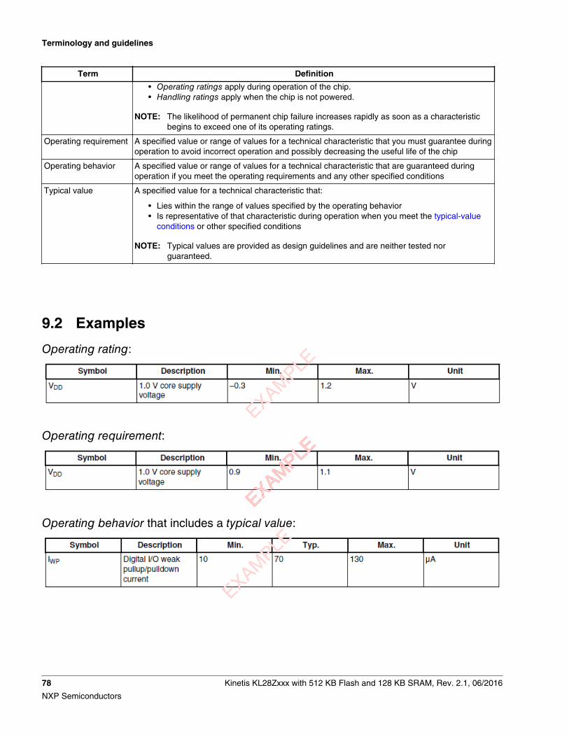
Term Definition
• Operating ratings apply during operation of the chip.• Handling ratings apply when the chip is not powered.
NOTE: The likelihood of permanent chip failure increases rapidly as soon as a characteristicbegins to exceed one of its operating ratings.
Operating requirement A specified value or range of values for a technical characteristic that you must guarantee duringoperation to avoid incorrect operation and possibly decreasing the useful life of the chip
Operating behavior A specified value or range of values for a technical characteristic that are guaranteed duringoperation if you meet the operating requirements and any other specified conditions
Typical value A specified value for a technical characteristic that:
• Lies within the range of values specified by the operating behavior• Is representative of that characteristic during operation when you meet the typical-value
conditions or other specified conditions
NOTE: Typical values are provided as design guidelines and are neither tested norguaranteed.
9.2 Examples
Operating rating:
Operating requirement:
Operating behavior that includes a typical value:
EXAMPLE
EXAMPLE
EXAMPLE
EXAMPLE
Terminology and guidelines
78 Kinetis KL28Zxxx with 512 KB Flash and 128 KB SRAM, Rev. 2.1, 06/2016
NXP Semiconductors
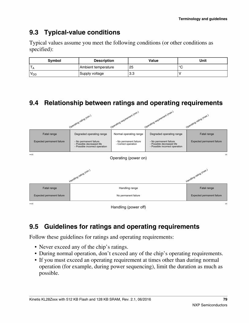
9.3 Typical-value conditions
Typical values assume you meet the following conditions (or other conditions asspecified):
Symbol Description Value Unit
TA Ambient temperature 25 °C
VDD Supply voltage 3.3 V
9.4 Relationship between ratings and operating requirements
–∞
- No permanent failure- Correct operation
Normal operating rangeFatal range
Expected permanent failure
Fatal range
Expected permanent failure
∞
Operating rating (max.)
Operating requirement (max.)
Operating requirement (min.)
Operating rating (min.)
Operating (power on)
Degraded operating range Degraded operating range
–∞
No permanent failure
Handling rangeFatal range
Expected permanent failure
Fatal range
Expected permanent failure
∞
Handling rating (max.)
Handling rating (min.)
Handling (power off)
- No permanent failure- Possible decreased life- Possible incorrect operation
- No permanent failure- Possible decreased life- Possible incorrect operation
9.5 Guidelines for ratings and operating requirements
Follow these guidelines for ratings and operating requirements:
• Never exceed any of the chip’s ratings.• During normal operation, don’t exceed any of the chip’s operating requirements.• If you must exceed an operating requirement at times other than during normal
operation (for example, during power sequencing), limit the duration as much aspossible.
Terminology and guidelines
Kinetis KL28Zxxx with 512 KB Flash and 128 KB SRAM, Rev. 2.1, 06/2016 79
NXP Semiconductors
10 Revision HistoryThe following table provides a revision history for this document.
Table 53. Revision History
Rev. No. Date Substantial Changes
0 08/2015 Initial release
1 10/2015 • Removed "Ready Play module (RPM)" from the features list• Added "96 MHz high speed mode" to the features list under "Core"• Updated the values in the following sections:
• Voltage and current operating requirements• Power mode transition operating behaviors• EMC radiated emissions operating behaviors• General switching specifications• Oscillator frequency specifications• 16-bit ADC operating conditions• LPSPI switching specifications• LPI2C specifications
• Created new table for topic "Power consumption operating behaviors"• Updated the pinouts• Updated the "Terminology and guidelines" section to a new format
2 04/2016 • Removed 64-pin package information and marked 121-pin package information as"Package Your Way"
• Updated the values in Power mode transition operating behaviors• Updated values and resolved TBDs in Power consumption operating behaviors• In section Diagram: Typical IDD_RUN operating behavior :
• Added "For the ALLON curve, all peripheral clocks are enabled as specified innotes of Table 9."
• Updated figures• Updated table in Slow IRC (SIRC) specifications• Removed section "Specification Test Methods"• In table VREF full-range operating behaviors, removed the user trim values and
updated the factory trim values
2.1 06/2016 • In table Table 10 Low power mode peripheral adders — typical value, removedIUSB_Alive
Revision History
80 Kinetis KL28Zxxx with 512 KB Flash and 128 KB SRAM, Rev. 2.1, 06/2016
NXP Semiconductors
How to Reach Us:
Home Page:nxp.com
Web Support:nxp.com/support
Information in this document is provided solely to enable system and softwareimplementers to use NXP products. There are no express or implied copyrightlicenses granted hereunder to design or fabricate any integrated circuits basedon the information in this document. NXP reserves the right to make changeswithout further notice to any products herein.
NXP makes no warranty, representation, or guarantee regarding the suitability ofits products for any particular purpose, nor does NXP assume any liability arisingout of the application or use of any product or circuit, and specifically disclaimsany and all liability, including without limitation consequential or incidentaldamages. “Typical” parameters that may be provided in NXP data sheets and/orspecifications can and do vary in different applications, and actual performancemay vary over time. All operating parameters, including “typicals,” must bevalidated for each customer application by customerʼs technical experts. NXPdoes not convey any license under its patent rights nor the rights of others. NXPsells products pursuant to standard terms and conditions of sale, which can befound at the following address: nxp.com/SalesTermsandConditions.
NXP, the NXP logo, NXP SECURE CONNECTIONS FOR A SMARTERWORLD, Freescale, the Freescale logo, and Kinetis are trademarks of NXP B.V.All other product or service names are the property of their respective owners.ARM, the ARM powered logo, and Cortex are registered trademarks of ARMLimited (or its subsidiaries) in the EU and/or elsewhere. All rights reserved.
© 2015 - 2016 NXP B.V.
Document Number MKL28Z512Vxx7Revision 2.1, 06/2016